In the evolving landscape of electronics, the demand for precision and efficiency in PCB manufacturing is paramount. Laser cutting plays a crucial role in this process. Dr. Emily Zhang, an expert in PCB technology, emphasizes, "Laser cutting enables intricate designs and enhances production speed." This highlights why laser cutting is used for PCB manufacturing.
As manufacturers look to stay competitive, adopting advanced technologies is essential. Laser cutting offers advantages such as precision, flexibility, and reduced waste. The ability to create complex geometries sets it apart from traditional methods. Companies aiming for higher quality and consistency often lean toward laser cutting.
However, the adoption process is not without challenges. Understanding the technology's intricacies requires time and investment. Some manufacturers may hesitate, fearing the transition could disrupt current workflows. Overall, while laser cutting shows great promise in PCB manufacturing, its implementation must be carefully planned and executed.
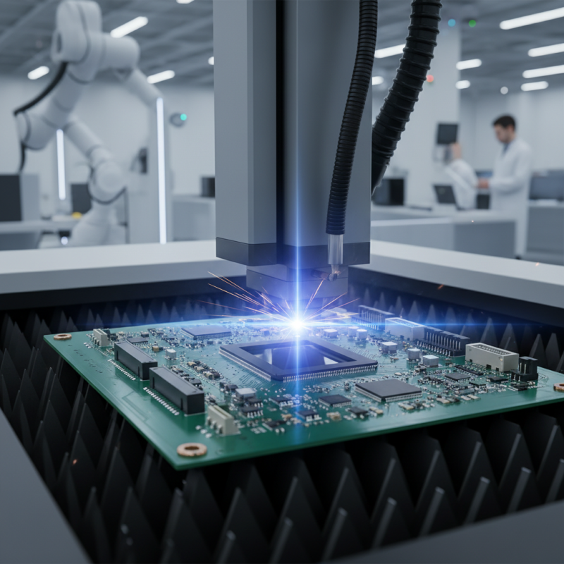
Laser cutting technology has transformed PCB manufacturing in recent years, making it a crucial element for the industry as we approach 2026. This method allows for precision cutting of intricate patterns on printed circuit boards. The high accuracy minimizes material waste and ensures that components fit perfectly. Traditional cutting techniques struggle with complex designs, leading to errors. In contrast, laser cutting achieves clean edges, enhancing the reliability of PCBs.
Another advantage of laser cutting is its ability to handle diverse materials. From flexible substrates to rigid boards, laser technology adapts well. It can easily switch between materials without significant downtime. Yet, there are challenges. The initial setup cost may deter some manufacturers. Additionally, new operators require training to ensure optimal use of the technology. Mistakes can arise from inexperience, impacting production flow.
Despite these hurdles, laser cutting remains essential for future PCB production. As electronics continue to shrink in size, the demand for precision increases. Companies must refine their techniques to stay competitive. Embracing laser cutting is not just about upgrading machinery; it’s about fostering expertise and addressing limitations head-on. The journey involves learning from each step, ensuring quality and efficiency in every cut.
Laser cutting is transforming PCB manufacturing. It offers precision that traditional methods cannot match. The ability to cut intricate designs with minimal material waste is a game changer. Traditional techniques often struggle with complex layouts, leading to inaccuracies. Laser cutting excels in this area. It allows for tighter tolerances and better-quality finishes.
The speed of laser cutting is another advantage. It significantly reduces production time. Manufacturers can respond quickly to customer demands. In contrast, traditional methods can be slow and labor-intensive. Additionally, laser cutting requires less manual intervention. This decreases the risk of human error and increases reliability.
However, some challenges exist. Initial costs for laser cutting equipment can be high. Not all manufacturers may have the resources for this investment. Training is necessary to operate these machines effectively. Despite these drawbacks, the benefits outweigh the limitations. The future of PCB manufacturing will likely revolve around laser technology, for those who can adapt.
Laser cutting is revolutionizing PCB manufacturing by introducing innovative applications that enhance design precision. This technology enables the creation of intricate patterns with remarkable accuracy. By utilizing focused laser beams, manufacturers can achieve complex geometries that traditional methods struggle to replicate. This capability results in more compact and efficient PCB designs, essential for modern electronic devices.
The advent of laser cutting also facilitates the use of new materials, broadening design possibilities. Designers can explore substrates that were previously difficult to use. This flexibility not only enhances performance but also impacts durability. However, the rapid pace of change prompts reflection on manufacturing standards. Ensuring quality control amid these advancements remains a challenge.
Moreover, integrating laser cutting into the workflow can lead to unforeseen complexities. As machine setups evolve, operators need to adapt quickly. There is a learning curve that must be addressed to fully leverage these benefits. Continuous training is vital to maintain expertise in this fast-evolving field. The balance between innovation and operational efficiency is crucial for long-term success.
| Application | Advantages | Key Technologies Used | Future Trends |
|---|---|---|---|
| High Precision Cutting | Minimized material wastage, finer tolerances | Fiber Lasers, CO2 Lasers | Increased automation in cutting processes |
| Complex Geometries | Ability to create intricate designs | Ultrafast Lasers | Integration with AI for design optimization |
| Layer Structure Creation | Efficient layer separation with micro features | Laser Micro-Machining | Advancements in laser scanning technologies |
| Surface Texturing | Enhanced adhesion for components | Pulsed Laser Systems | Innovative textures for better electrical performance |
| Prototype Development | Rapid turnaround for testing and iterations | Dynamic Laser Cutting Systems | On-demand manufacturing capabilities |
Laser cutting has become a transformative technology in PCB manufacturing. It significantly enhances production efficiency and cost-effectiveness. Precision is crucial in this field, and laser cutting excels here. It allows for intricate designs and detailed features that traditional methods struggle to achieve. The accuracy of laser cutting minimizes errors. This leads to fewer reworks and lower waste rates.
Production timelines benefit from laser cutting as well. The speed at which lasers operate reduces manufacturing time. Quick turnaround on projects is essential for companies to stay competitive. While most manufacturers recognize these benefits, the adoption rate varies. Some still rely on outdated methods. They may not realize how their processes impact overall costs.
However, it is important to consider the investment. The initial setup for laser cutting can be high. Companies must weigh these costs against potential savings. Evaluating this balance is necessary for sustainable growth. In the rapidly evolving landscape of PCB manufacturing, embracing technology like laser cutting is not just beneficial; it is essential.
As PCB manufacturing evolves in 2026, laser cutting is set to play a pivotal role. This technology allows for precise cuts and intricate designs, which are essential for modern electronics. With the increasing demand for miniaturization, laser cutting provides the accuracy needed for smaller components. Manufacturers are leveraging this method to enhance production efficiency and reduce waste.
Future trends indicate that laser technology will become even more integral. It streamlines processes and increases flexibility in design changes. Additionally, advancements in laser systems will allow for more complex geometries in PCBs. However, the challenge of integrating this technology into existing workflows remains. Some manufacturers may struggle with the initial investment or training.
The potential for laser cutting to revolutionize PCB manufacturing is clear. Yet, careful consideration is required to ensure its successful implementation. Balancing technology adoption with practical workflows is crucial for maximizing benefits. This balancing act will define the future of PCB manufacturing in the coming years.
: Laser cutting technology allows for precise cuts on printed circuit boards, making it vital for the industry.
It minimizes material waste and ensures that components fit perfectly, enhancing reliability and accuracy.
Laser technology can handle flexible substrates and rigid boards, adapting well without significant downtime.
Initial setup costs can be high, and operators require training to use the technology effectively.
Inexperienced operators may make mistakes, which can disrupt production flow and impact overall efficiency.
Laser cutting offers tighter tolerances, better finishes, and faster production times than traditional methods.
High initial costs and the need for expert training may deter some manufacturers from adopting this technology.
As demand for miniaturization grows, laser cutting will become more integral for producing complex PCB designs.
Balancing technology adoption with practical workflows is crucial for maximizing benefits in PCB manufacturing.
Companies must refine techniques and foster expertise to stay competitive in an evolving landscape.
In 2026, laser cutting technology has become integral to PCB manufacturing due to its precision and efficiency. This method streamlines the production process, allowing for intricate designs that traditional fabrication techniques cannot achieve. The advantages of laser cutting include faster turnaround times, reduced material waste, and the ability to handle complex geometries, answering the question of why laser cutting is used for PCB manufacturing.
Innovative applications of this technology are evident in advanced PCB designs, supporting the demand for miniaturization and increased functionality in electronics. As production efficiency and cost-effectiveness continue to improve, laser cutting is positioned to lead the future trends in PCB manufacturing, reflecting its critical role in adapting to the evolving needs of the industry.
Focus Laser