The rapid evolution of technology has significantly impacted various industries, including printed circuit board (PCB) manufacturing. As we look ahead, many professionals ponder, "what is the future of PCB laser technology?" This question taps into the heart of innovation and efficiency in PCB production. Laser technology is not just a trend; it is reshaping how we approach design, prototyping, and production processes.
Experts in the field highlight the potential for increased precision and speed. Laser technology offers advantages like smaller feature sizes and reduced material waste. However, there are challenges to address. Companies must consider the costs of implementing advanced laser systems. Additionally, there’s a learning curve for technicians adapting to new methods.
The future of PCB laser technology promises significant advancements. Yet, we must reflect on its limitations. Society sometimes overlooks the environmental impact of such technologies. Balancing innovation with sustainability will be crucial as we advance. Understanding these dynamics can inform better decisions for the future.
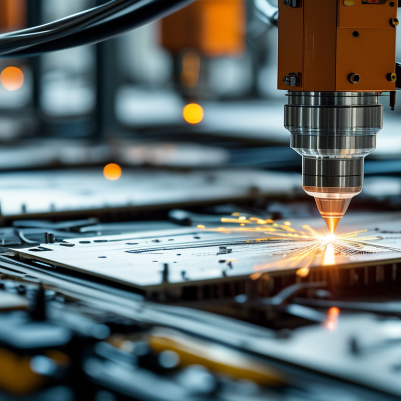
The future of PCB laser technology is bright and dynamic. As manufacturers seek efficiency, lasers provide precise etching and cutting. This trend will likely reduce production times and waste. Companies are looking for lightweight, flexible materials. Lasers can accommodate these demands well, enabling creativity in design.
One key insight is the growing adoption of automation in PCB production. This move not only enhances accuracy but also lowers human error. However, the investment in advanced laser systems can be costly. Smaller firms might struggle with funding, affecting their competitiveness. Research indicates that the technology is rapidly evolving. Expect to see developments in laser wavelengths that enhance material processing capabilities.
Furthermore, sustainability is becoming crucial in the industry. Eco-friendly practices are being prioritized by many companies. However, integrating these practices with advanced laser technology remains a challenge. Companies must adapt or risk falling behind. The balance between innovation and cost is delicate. Future success will depend on navigating these complexities effectively.
The landscape of printed circuit board (PCB) laser technology is evolving rapidly in 2023. Key innovations are reshaping the industry. A recent market report indicates that the global PCB laser market is projected to grow at a CAGR of 8.5% from 2023 to 2028. This growth is driven by demand for efficient manufacturing processes and miniaturization in electronic components.
One significant advancement is the rise of ultra-fast laser systems. These lasers enable precise micro-drilling and minimal thermal impact. Research shows that using ultra-fast lasers can reduce material waste by nearly 30%. This efficiency not only lowers costs but also promotes sustainability in PCB production. Moreover, advancements in software that optimize laser parameters are enhancing accuracy. These tools empower designers to achieve intricate patterns that were previously unattainable.
Challenges remain, however. While laser technology improves, integration with existing systems can be complex. Many manufacturers face a steep learning curve in adopting these innovations. Furthermore, quality control must keep pace with new technologies. Ensuring reliability is paramount in high-stakes applications such as automotive and aerospace. The future of PCB laser technology hinges on overcoming these hurdles while embracing new techniques.
Laser technology has revolutionized PCB manufacturing, enhancing both efficiency and precision. Traditionally, drilling and cutting methods often resulted in inaccuracies. However, lasers deliver high precision, cutting through materials with minimal thermal impact. This means fewer errors and better-quality boards in a fraction of the time.
The precision of laser machining allows manufacturers to create finer traces and smaller vias. This capability is crucial for the growing demand for compact electronic devices. Yet, the transition to laser technology is not without challenges. High initial costs and the need for specialized training can hinder some manufacturers. Many workers need time to adapt to new processes and techniques.
Moreover, while laser technology boosts efficiency, its implementation requires careful planning. The wavelength and power settings must be meticulously calibrated for different materials. Overlooking these details can lead to defects or inconsistent results. Ultimately, the impact of laser technology on PCB manufacturing is significant, but its complexities require ongoing consideration and adjustment.
Laser technology is revolutionizing PCB production. Traditional methods rely heavily on mechanical processes, which can be slower and less precise. Recent studies indicate that laser processing can enhance efficiency by up to 50%. This improvement comes from the ability of lasers to make highly accurate cuts without physical contact.
With traditional methods, manufacturers often face limitations. The wear on tools can lead to inconsistent quality. In contrast, laser processing offers reliable precision across various materials. A study shows that the laser's ability to adjust pulse settings results in cleaner edges and finer details, significantly reducing the need for further post-processing.
However, challenges still exist. The initial setup costs for laser systems can be high, which may deter smaller manufacturers. Additionally, while lasers excel in precision, they may struggle with certain thicker substrates. This balance between upfront investment and long-term efficiency needs careful consideration. As the industry evolves, ongoing research will determine the best practices for integrating laser technology into PCB production.
| Aspect | Traditional Processing | Laser Processing |
|---|---|---|
| Speed | Moderate | High |
| Accuracy | Good | Excellent |
| Material Versatility | Limited | High |
| Setup Time | Long | Short |
| Cost | Lower | Higher |
| Waste Generation | Higher | Lower |
| Scalability | Moderate | High |
Integrating laser technology into PCB manufacturing presents both challenges and opportunities. One major challenge is the precision required for intricate designs. Laser systems must achieve high accuracy to prevent defects. This precision often demands expensive and complex machinery. Not every manufacturer can afford this investment.
On the opportunity side, laser technology significantly enhances efficiency. It reduces material waste and allows for faster production times. Flexible designs become more feasible, leading to innovation in PCB applications. However, training staff to operate advanced laser equipment can be daunting. The learning curve poses a barrier for many businesses.
Despite these challenges, adapting to laser technology can yield competitive advantages. Companies that invest in this integration may find long-term benefits. They could lead in the ever-evolving electronics market. Pushing through challenges can pave the way for breakthroughs in PCB design and functionality.
: Lasers enhance efficiency, reduce production times, and minimize waste. They provide precise etching and cutting.
Lasers can improve efficiency by up to 50%. Traditional methods may lead to inconsistent quality due to tool wear.
Yes, integration can be complex. Many manufacturers face a learning curve when adopting new laser systems.
Innovations include ultra-fast laser systems that enable precise micro-drilling and enhance material processing capabilities.
Many companies are prioritizing eco-friendly practices, but integrating these with laser technology remains a challenge.
High initial setup costs can deter smaller firms, potentially impacting their competitiveness in the market.
Using ultra-fast lasers can reduce material waste by nearly 30%, promoting sustainability in the production process.
Accuracy is critical for high-stakes applications like automotive and aerospace, ensuring reliability and safety.
Software optimizes laser parameters, enhancing accuracy and allowing designers to create intricate patterns.
Yes, companies must navigate the delicate balance between investing in innovation and managing costs effectively.
The future of PCB laser technology holds significant promise, driven by current market insights and innovative advancements in 2023. Key innovations are enhancing manufacturing efficiency and precision, transitioning the industry from traditional methods to laser processing. This shift enables more intricate designs and faster production times, ultimately appealing to the growing demand for high-performance electronics.
However, what is the future of PCB laser technology also involves navigating challenges such as integration issues and the need for skilled professionals. Despite these hurdles, the comparative advantages of laser technology over conventional processing methods highlight its potential to revolutionize PCB manufacturing. As industries continue to adapt, there remains ample opportunity for growth and development in this dynamic field.
Focus Laser