1 / 5
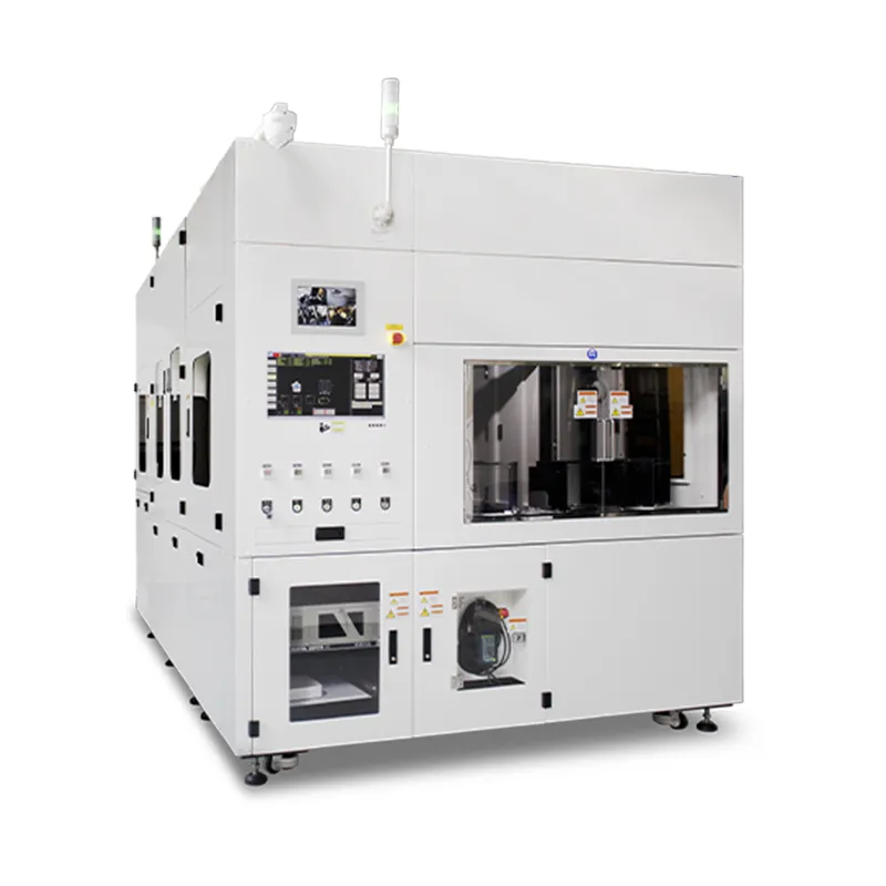
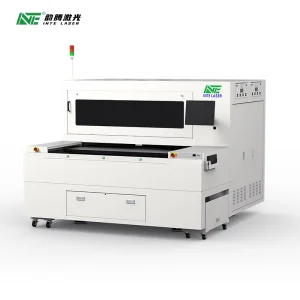
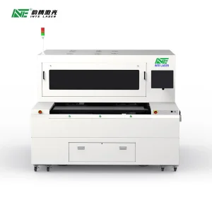
Debonding of temporary bonded wafer by laser, followed by separating, and cleaning, for carrier substrate re-use and ultra-thin wafer subsequent processing.
| Technical Specification | |
|---|---|
| Laser wavelength | 355nm/1340nm |
| Wafer size | 6 inch, 8 inch, 12 inch |
| Laser power | 15/30W@355nm, 100W@1340nm |
| Focused spot size | X:0.2mm~1.0mm, Y:0.2mm~1.0mm |
| Laser energy density | 0.05-1J/cm² |
| Typical Laser Scan Time | 100 sec@12 inch |
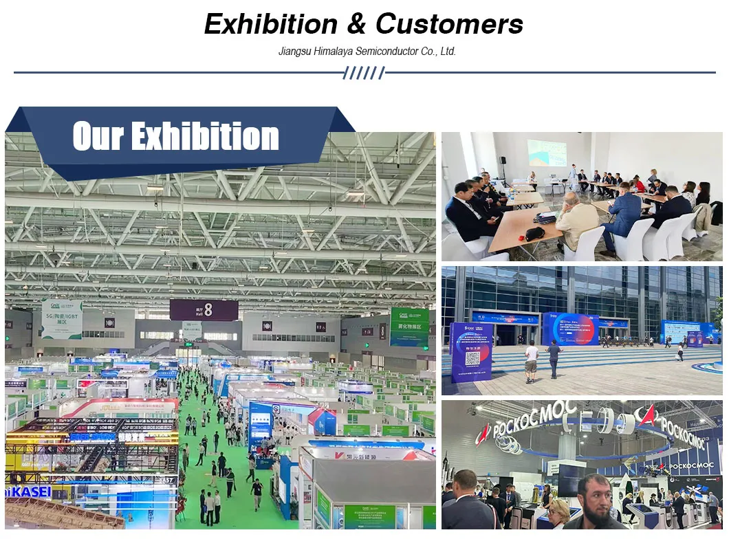
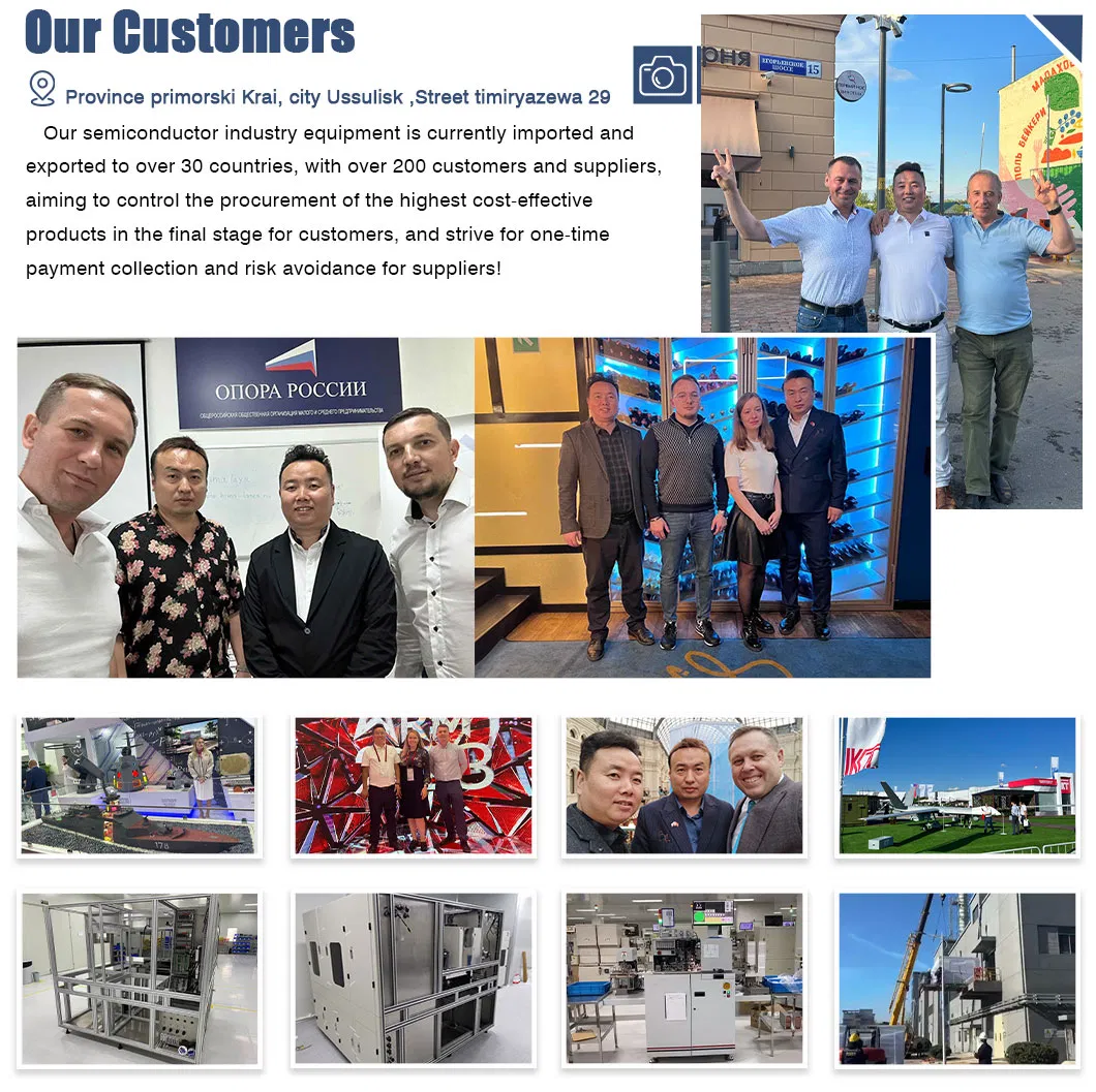
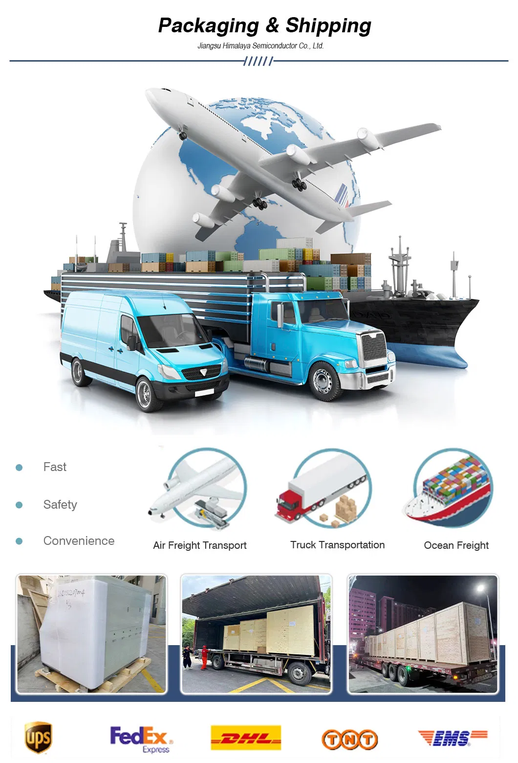
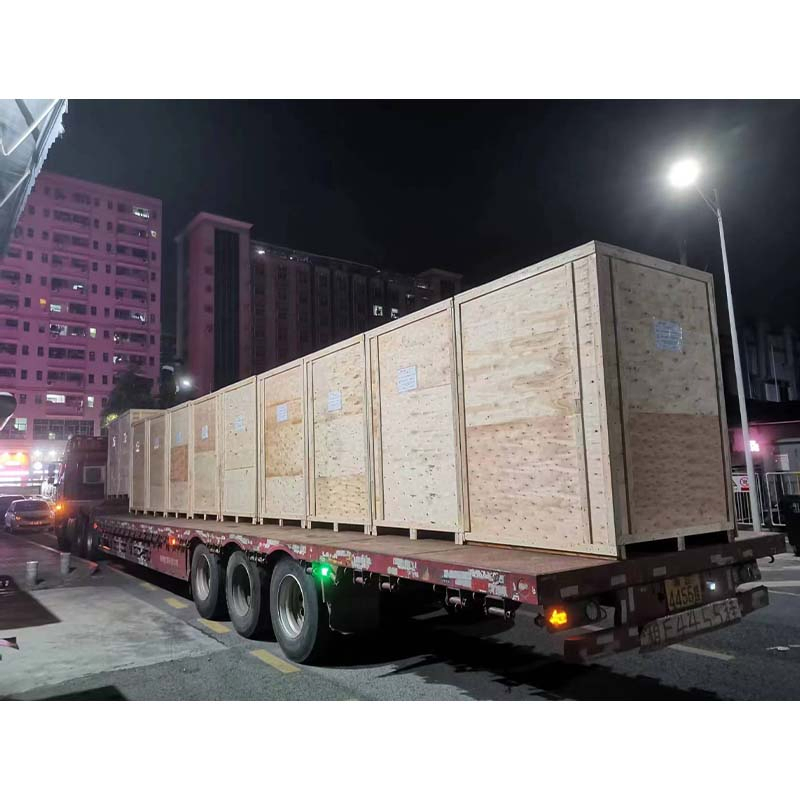
Our focus is on international trade and integration of semiconductor industry equipment. We serve customers in over 30 countries with a robust network of over 200 customers and suppliers, ensuring high cost-effectiveness and risk avoidance.
Core Product Portfolio: Die Bonder, Wire Bonding, Laser Marking (ID IC Wafer), Laser Grooving, Laser Cutting (Glass Ceramics Wafers Packaging), Laser Internal Modification Machines (Si/SiC, LT/LN Wafers), Laser Annealing Machines, Automatic Dicing Saw Machines, and Automatic Silicone Dispensing Equipment.