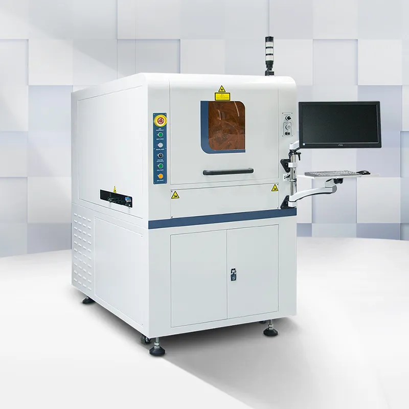
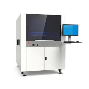
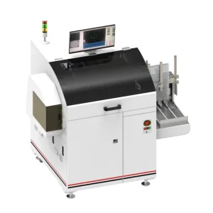
Advanced Precision Marking Solutions for PCBA and IC Production

Customization: Available
After-sales Service: Provided
Warranty: Provided

Product Description

⚙️ Basic Information
Product Name
PCBA & IC & Wafer Marking Machine
Laser Visibility
Visible
Applicable Material
Metal
Laser Wavelength
UV Laser, CO2 Laser
Laser Classification
Semiconductor Laser
Trademark
Himalaya
Origin
China
Transport Package
Customized or Wooden Box Packaging
📦 Product Description
🔍 PCBA & IC & Wafer Marking Solutions
Marking Machine

Brief Description:

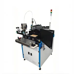
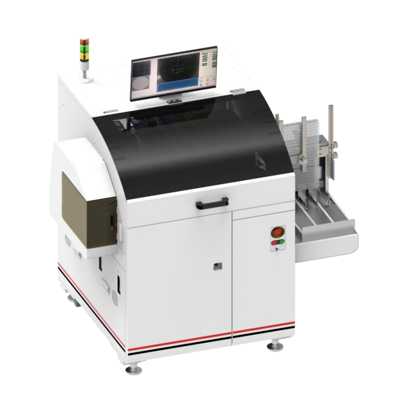
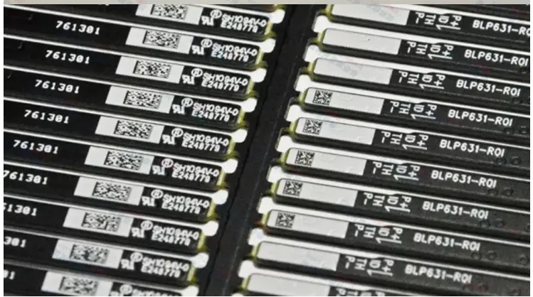
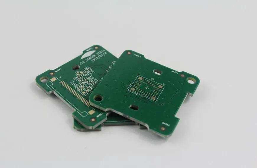
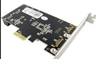
Applicable for digital products, wearable devices, automobile PCBA, mobile phone PCBA, FPC, and more. Highly efficient for marking on Rigid and flexible printed circuit boards (PCBAs). Supports 1D barcodes, 2D Matrix, QR codes, logos, and batch number marking.

Key Features
  • Fully-automatic loading and unloading from hanging basket to hanging basket, stable laser output, and intelligent vision system for direction and sampling inspection.
  • Friendly HMI (Human-Machine Interface) for ease of operation.
  • Imported double-head 20W fiber laser marking system; Green, UV, and CO2 laser sources are optional.
  • Equipped with a special fume removal device to protect the marking area and environment.
  • Full compliance with CE MARK and SEMI standards.
📊 Technical Specifications
Parameter HDZ-SIC100 HDZ-SIC200
Marking scope 320mm*160mm 320mm*160mm
Product specification L: 160-320mm; W: 30-80mm L: 160-320mm; W: 30-80mm
Font TFT and SHX; with font library module modification program
Repeated Positioning Precision ±0.1mm ±0.1mm
UPH 1200 pieces/h (idle) 1200 pieces/h (idle)
Power supply AC 220V, 50/60Hz AC 220V, 50/60Hz
Air source 0.6-0.8 MPa 0.6-0.8 MPa
Overall dimension 2525mm*1665mm*2000mm 2515mm*1420mm*2000mm
🤝 Exhibition & Customers

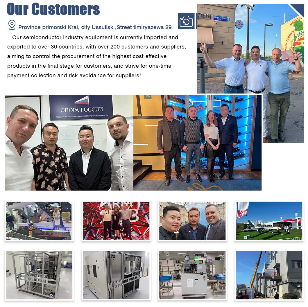
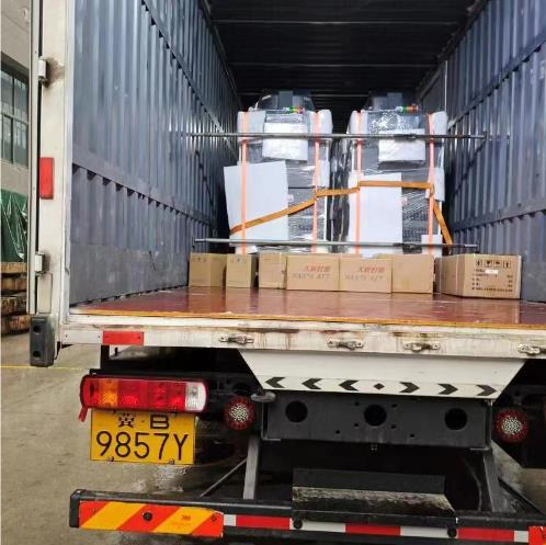
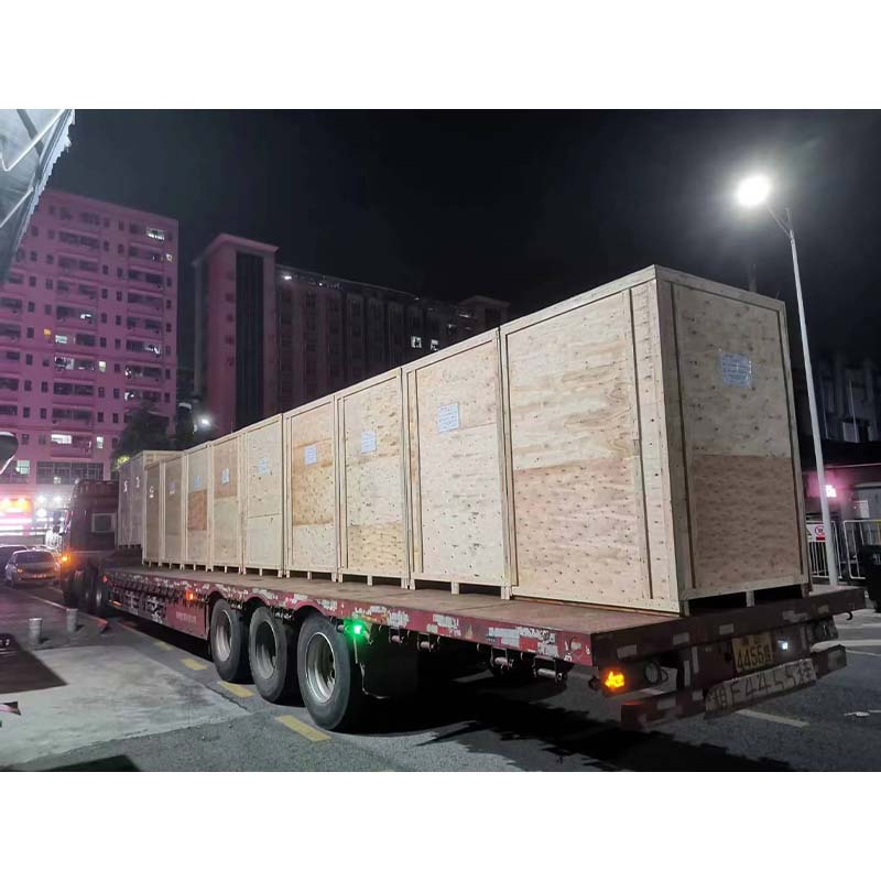
Our equipment is currently imported and exported to over 30 countries, with over 200 customers and suppliers. We aim to control the procurement of the highest cost-effective products for customers, ensuring reliable payment collection and risk avoidance.

Main Product Line: Die Bonder, Wire Bonding, Laser Marking (ID IC Wafer), Laser Grooving, Laser Cutting (Glass Ceramics Wafers Packaging), Laser Internal Modification Machines (Si/Sic, Lt/Ln Wafer), Laser Annealing Machines, and Automatic Dicing Saw Machines.

🚢 Packaging & Shipping
Packaging and Shipping
Frequently Asked Questions
Q1: How to choose a suitable machine?
A1: You can tell us the working piece material, size, and the requested machine functions. We will recommend the most suitable configuration based on our extensive industry experience.
Q2: What is the warranty period for the equipment?
A2: We provide a one-year warranty along with 24-hour online professional technical support to ensure your production remains uninterrupted.
Q3: Why choose our marking solutions?
A3: We offer comprehensive OEM/ODM services and custom design capabilities tailored to your specific semiconductor and PCBA production needs.
Q4: What is the lead time for a standard machine?
A4: Lead times typically range from 4 to 8 weeks depending on the level of customization and current production schedule.
Q5: Is on-site training provided for the marking machines?
A5: Yes, we provide detailed video tutorials and remote training. On-site installation and training by our engineers can also be arranged upon request.
Q6: Do you support international shipping and customs clearance?
A6: We have extensive experience exporting to over 30 countries and provide full support for international logistics and necessary documentation.

Related Products