Hangzhou Focus Laser Co., Ltd. stands as a beacon of innovation in the global laser processing landscape. As a premier manufacturer specializing in advanced laser equipment for the electronics and display sectors, we have redefined the standards for PCB laser cutting and glass laser processing.
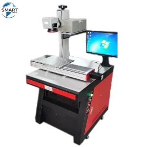
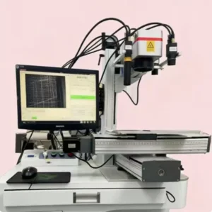
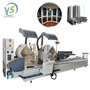
Our core competency lies in the seamless integration of ultra-fine beam control, high-speed CNC systems, and intelligent CCD vision alignment. This synergy allows us to deliver solutions that cater to the most demanding micro-electronics manufacturing environments, including semiconductor packaging and high-density flexible circuit board (FPC) processing.
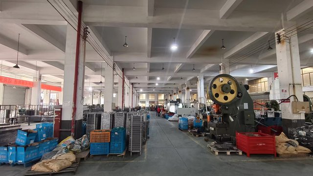
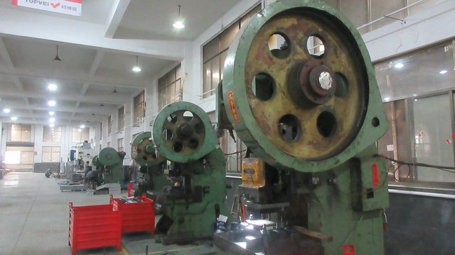
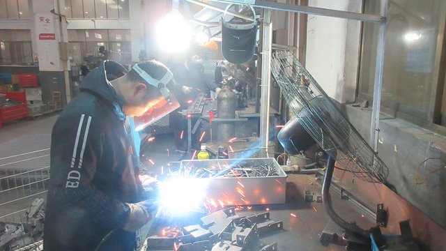
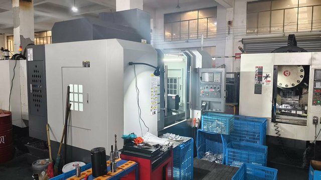
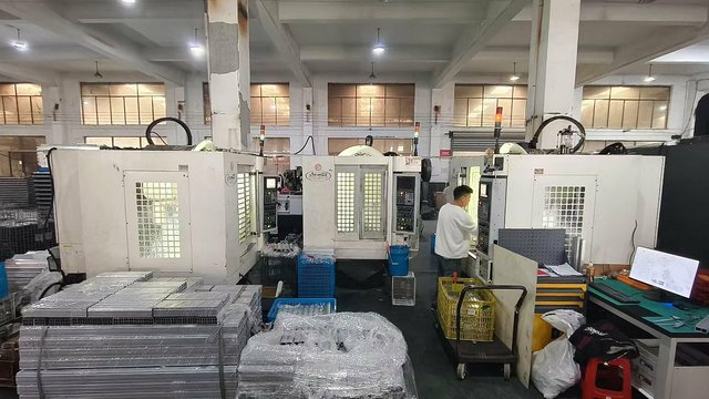
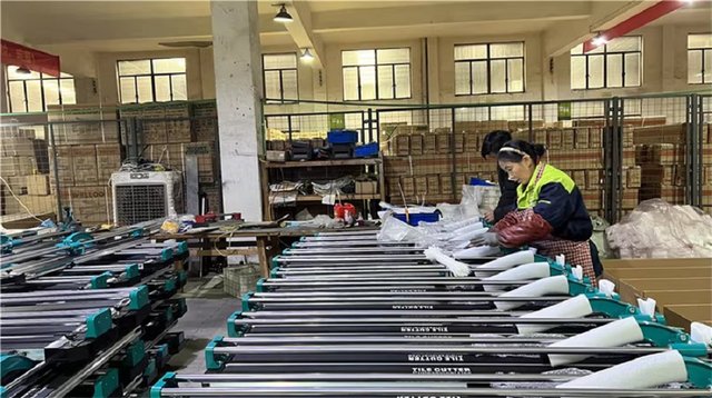
Located in the heart of China's tech hub, we leverage a robust ecosystem of high-end optical components and precision mechanical suppliers, ensuring rapid prototyping and scalable production.
Our engineering team provides rapid OEM/ODM iterations. We can transition from a client's specific requirement to a functional prototype 40% faster than traditional Western manufacturers.
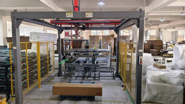
By optimizing manufacturing workflows and utilizing advanced CNC automation, we provide Tier-1 laser technology at a competitive price point without compromising on E-E-A-T standards.
The rise of 5G communications, IoT devices, and foldable smartphone displays has pushed Flexible Printed Circuits (FPC) to their physical limits. Traditional mechanical die-cutting is no longer viable for high-density interconnects due to physical stress and burrs. This is where laser technology becomes indispensable.
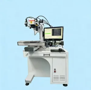
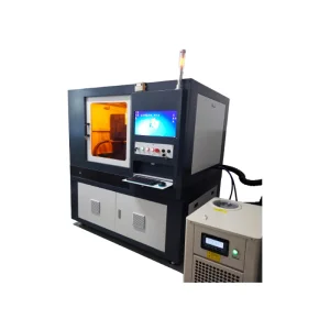
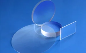
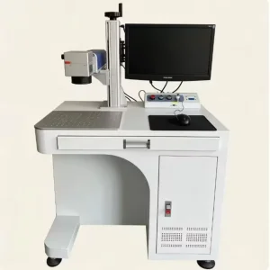
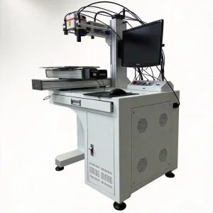
UV Laser vs. Picosecond Laser: For standard FPC depaneling, 355nm UV lasers offer a "cold" cutting process, minimizing the Heat Affected Zone (HAZ). However, for ultra-thin semiconductors and sapphire glass, our Picosecond systems provide sub-micron precision, effectively vaporizing material before heat can transfer to the substrate.
The Shift to Automation: Modern production lines demand zero-defect manufacturing. Our equipment integrates AI-driven CCD Vision systems that automatically compensate for material deformation in real-time, ensuring every cut is perfectly aligned with the circuit patterns.
Sustainability in Manufacturing: Laser processing is inherently cleaner than chemical etching or mechanical milling. It reduces waste, eliminates the need for expensive dies, and lowers the overall carbon footprint of the electronics assembly process.
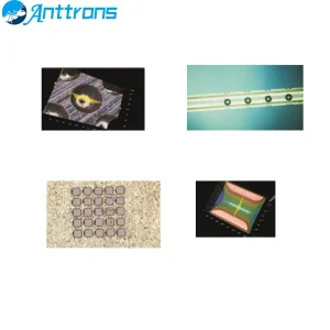
High-speed cutting of FPC for smartphone camera modules, battery protection boards, and OLED screen connectors.
Processing of durable flexible circuits for EV battery management systems (BMS) and smart dashboard displays.
Micro-machining of biocompatible materials and ultra-small sensors used in wearable health monitors and implants.
Precision drilling and cutting of high-frequency LCP (Liquid Crystal Polymer) materials for satellite communication arrays and radar systems.
Our high-end UV and Picosecond systems achieve a positioning accuracy of ±2μm and a cutting repeatability of ±5μm, depending on the material thickness and type.
Yes, we offer comprehensive OEM services including custom chassis colors, software UI localization, and private labeling for established global distributors.
We utilize short-pulse UV laser sources and optimized scan strategies (burst mode) to ensure that thermal energy is dissipated before it can cause carbonization or delamination of the FPC layers.
Standard systems are shipped within 4-6 weeks. Highly customized ODM solutions typically require 8-12 weeks for R&D, assembly, and rigorous stress testing.