Advanced systems engineered for the North Korean industrial modernization and global electronics manufacturing.
Executive Summary: As global electronics shift toward miniaturization and high-frequency performance, High-Density Interconnect (HDI) PCBs have become the backbone of modern hardware. In regions like North Korea (DPRK), where industrial modernization and domestic technological self-reliance are prioritized, the acquisition of advanced laser via drilling systems represents a critical leap in manufacturing capability. This report explores the technical nuances, market dynamics, and the competitive advantage of Chinese laser technology in this specialized sector.
The Democratic People's Republic of Korea (DPRK) has shown a sustained interest in developing its domestic "CNC technology" and electronic manufacturing sectors. Key industrial hubs, such as the Pyongyang Information Center and various Special Economic Zones (SEZs), are increasingly focusing on telecommunications hardware, tablets, and specialized industrial controllers. To support these ambitions, the transition from standard multilayer PCBs to HDI PCBs is essential. HDI technology allows for more components per square inch, reducing device weight while increasing signal speed.
Exporting HDI PCB Laser Via Drilling Systems to North Korean enterprises involves understanding the local emphasis on Juche-oriented industrial growth, where high-efficiency, low-waste machinery from reliable neighbors like China plays a pivotal role. Our systems provide the necessary "Information Gain" by offering integrated software solutions that simplify the complex microvia drilling process, making high-tech production accessible to local engineering teams.
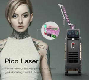
Mechanical drilling reaches its physical limits at around 150 microns. To achieve the sub-75 micron microvias required for 5G, IoT, and high-performance computing, laser technology is the only viable path. Our systems utilize UV and CO2 laser sources to create "blind" and "buried" vias with extreme thermal control.
As a premier manufacturer based in Hangzhou, China, Hangzhou Focus Laser Co., Ltd. offers a unique value proposition for the North Korean market and global buyers:
The application of HDI PCB laser drilling extends beyond simple consumer electronics. In the context of North Korean industrial needs, our systems serve:
Global enterprises looking to source or export to complex markets require a partner who understands the nuances of trade compliance, technical documentation, and localized training. Hangzhou Focus Laser provides comprehensive OEM/ODM services, ensuring that every system shipped is tailored to the specific voltage, language, and regulatory requirements of the destination country, including specialized documentation for industrial zones in North Korea.
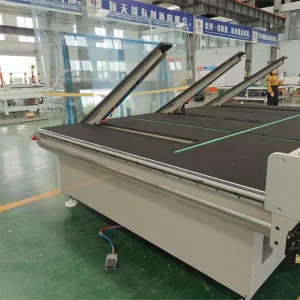
Professional manufacturer specializing in advanced laser processing equipment for the electronics and display industries. The company focuses on the development and production of PCB laser cutting machines and glass laser cutting systems, delivering high-precision solutions for micro-electronics manufacturing and optical material processing.
By integrating fiber laser technology and intelligent CNC systems, we ensure high cutting accuracy and minimal thermal damage, aiming to be the leading global supplier of precision laser solutions.
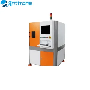
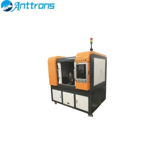
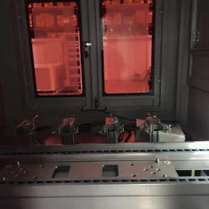
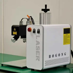
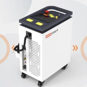
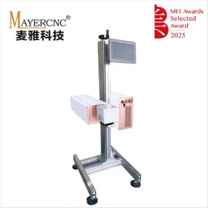
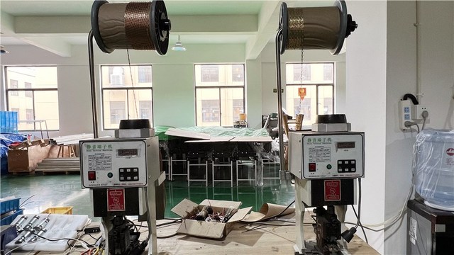
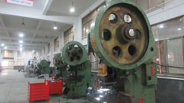
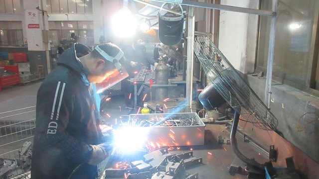
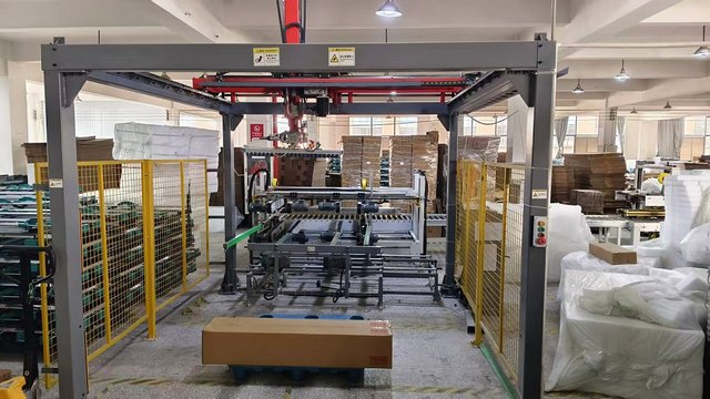
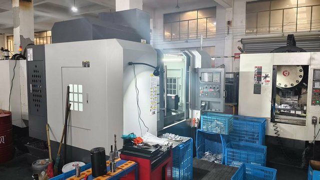
Get Technical SpecsReal-world applications of our laser drilling and cutting systems in high-tech facilities.

Our systems can achieve densities exceeding 10,000 holes per minute depending on the material substrate, with hole-to-hole accuracy maintained within +/- 10 microns, making them ideal for the most compact smartphone PCB designs found in the North Korean market.
We provide a multi-layered support strategy including remote diagnostic software, comprehensive video training modules, and on-site engineering support through our specialized regional export team, ensuring 99% machine uptime.
Yes, our UV laser systems are specifically designed for cold-ablation, which is perfect for FPC and Rigid-Flex boards, preventing the melting of Polyimide substrates common in modern wearable electronics.
From cleaning and welding to high-speed drilling and marking.