As the global electronics sector continues to shrink and optimize, Semiconductor Packaging Laser Cutting Solutions have emerged as the backbone of modern efficiency. Hangzhou Focus Laser Co., Ltd. stands at the forefront of this revolution, providing high-precision machinery that is transforming the manufacturing landscape. While Burundi is currently in a phase of strategic industrial development and infrastructure expansion, the integration of advanced manufacturing technologies like laser cutting represents a pivotal opportunity for local firms to upgrade their capabilities in electronics repair, solar panel assembly, and sustainable energy infrastructure.
Burundi is increasingly focusing on digital transformation and technical capacity building. By adopting or importing technologies that utilize advanced laser cutting, local enterprises in East Africa can leapfrog traditional, inefficient manufacturing methods. Whether it is precision marking for localized PCBA production or the utilization of custom aluminum profiles for machine guarding, these tools offer durability, precision, and scalability—essential pillars for any emerging industrial economy.
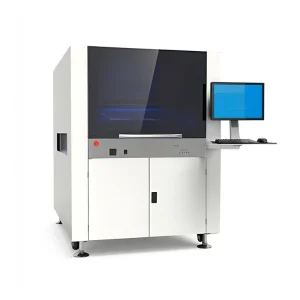
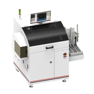
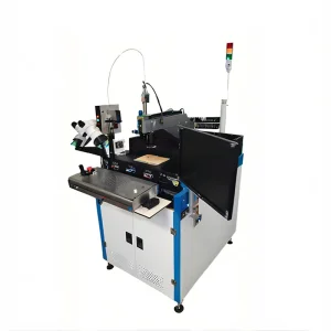
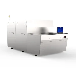
Hangzhou Focus Laser Co., Ltd. is a professional manufacturer specializing in advanced laser processing equipment for the electronics and display industries. The company focuses on the development and production of PCB laser cutting machines and glass laser cutting systems, delivering high-precision solutions for micro-electronics manufacturing and optical material processing.
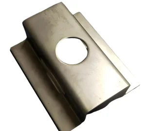
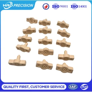
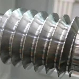
Its technologies are widely applied in PCB depaneling, flexible circuit board processing, semiconductor packaging, and precision glass cutting for smartphones, display panels, and optical components. By integrating fiber laser technology, ultra-fine beam control, and intelligent CNC systems, Hangzhou Focus Laser ensures high cutting accuracy, smooth edges, and minimal thermal damage during processing.
The company’s equipment is extensively used in industries such as consumer electronics, semiconductor manufacturing, automotive electronics, and smart display production. It supports both high-volume industrial production and customized precision machining requirements, ensuring that clients worldwide—including those in emerging markets—receive robust, industrial-grade machinery.
The trend towards miniaturization in semiconductor packaging is relentless. As devices become smaller and more integrated, the need for 'non-contact' laser processing becomes paramount. Traditional mechanical cutting is often too harsh for fragile semiconductor materials, causing micro-cracks and stress. Laser cutting, by contrast, operates with localized heating, ensuring structural integrity and longevity of the packaging materials.
Furthermore, as sustainability becomes a global mandate, the efficiency of laser cutting—reducing material waste and energy consumption—aligns perfectly with modern environmental, social, and governance (ESG) goals. For exporters and distributors targeting international markets, emphasizing this efficiency is key to building trust and authority.
Hangzhou Focus Laser Co., Ltd. is committed to engineering excellence, offering robust R&D, strict quality control, and unparalleled OEM/ODM support. Contact us today to discuss how our semiconductor packaging laser solutions can be adapted for your specific industrial needs, whether in Burundi or across the globe.
Send Inquiry Now