
1 / 5
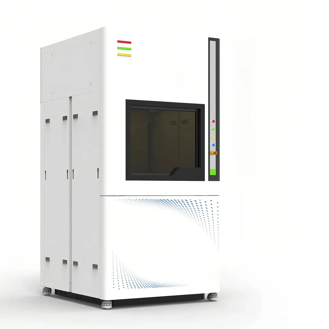
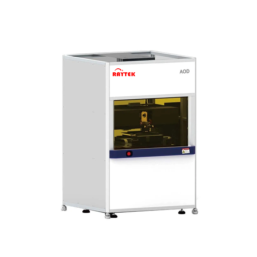
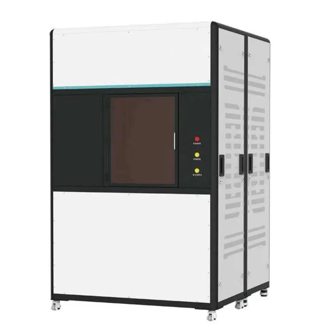
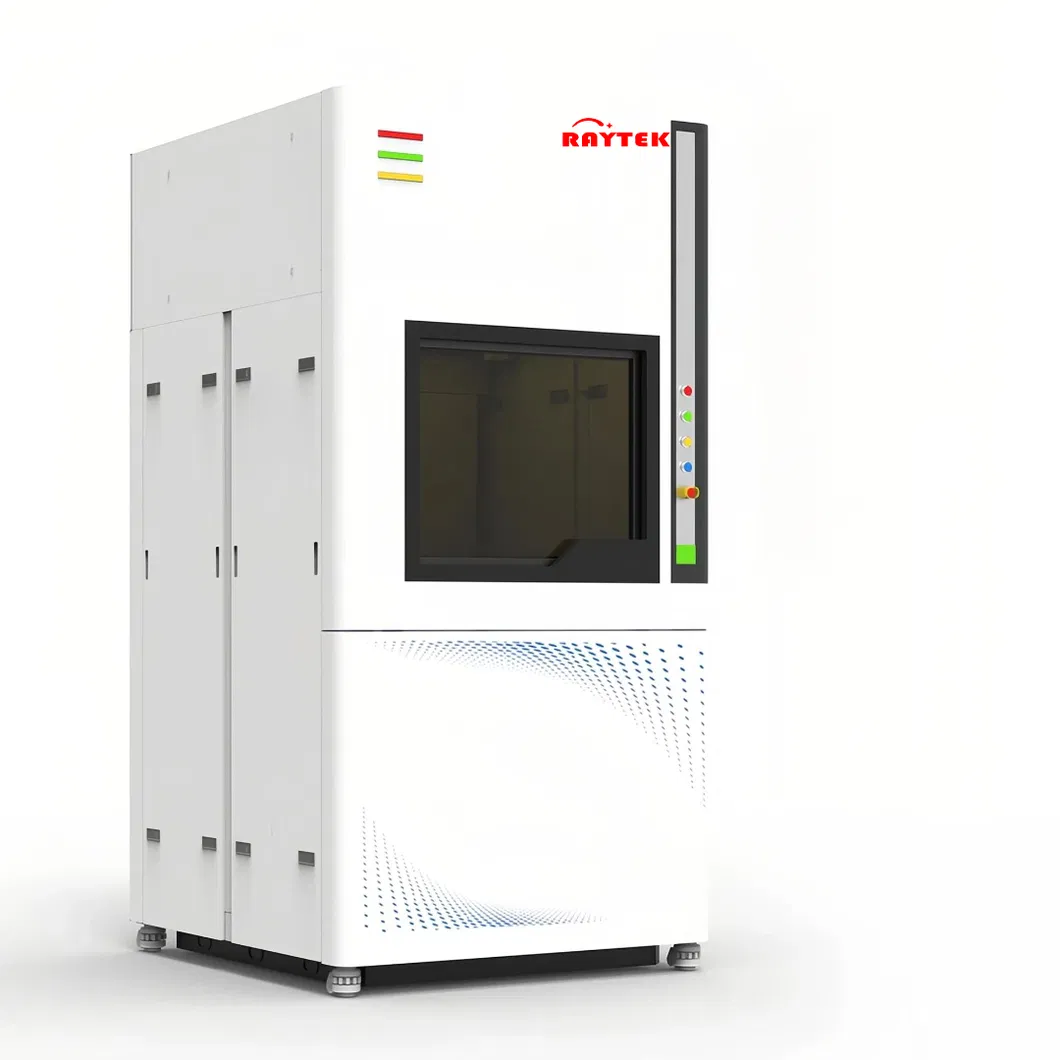
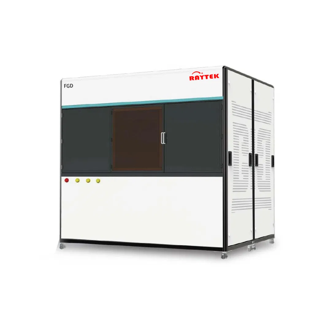
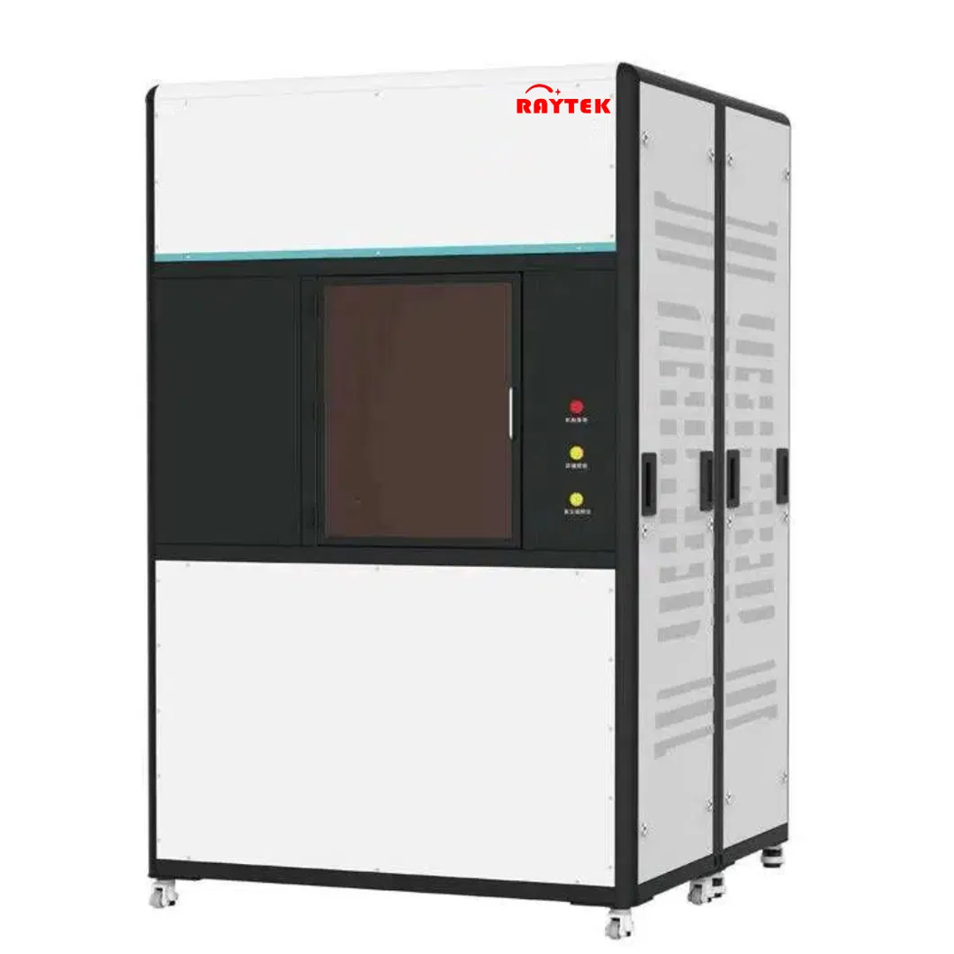
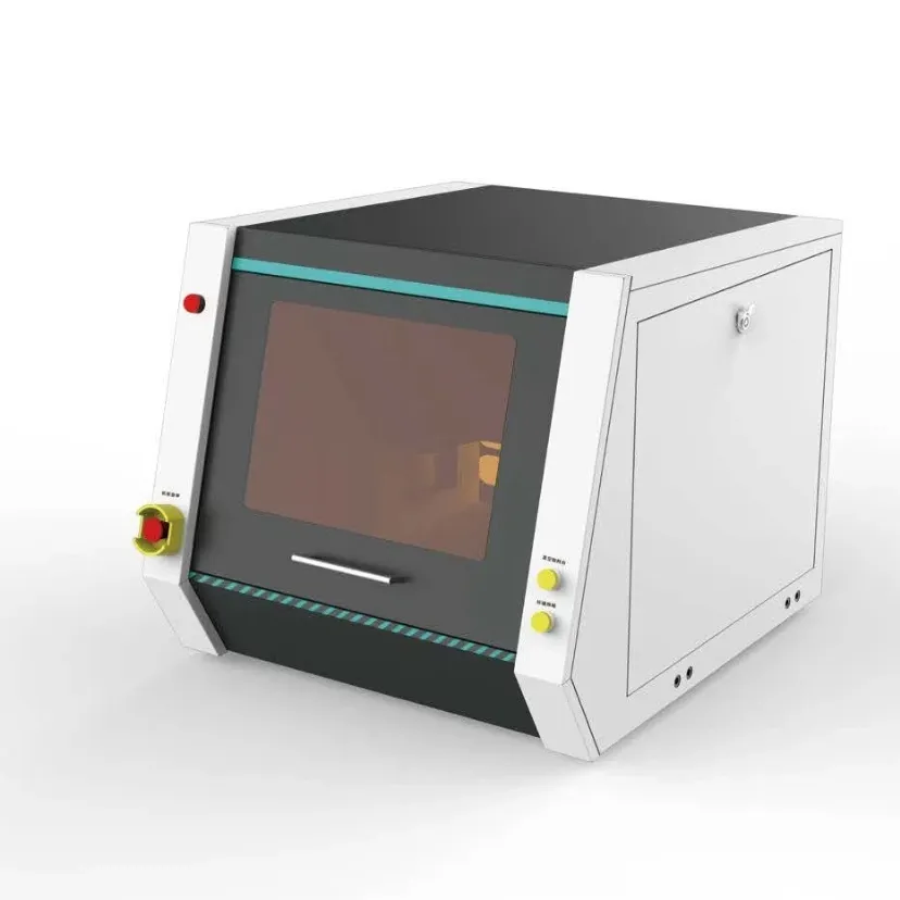
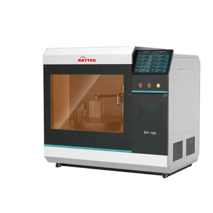
MPD Multi-Photon 3D Laser Direct-Write Photolithography System

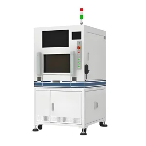
The MPD Series represents the pinnacle of maskless lithography technology, enabling nanometer-scale 3D structure fabrication with minimum feature sizes down to 50 nm. It breaks through the optical diffraction limit, delivering stable high-precision processing below 50 nm, providing advanced 3D manufacturing solutions for cutting-edge research and industrial applications.

| Parameter Category | Specification |
|---|---|
| System Parameters | Details |
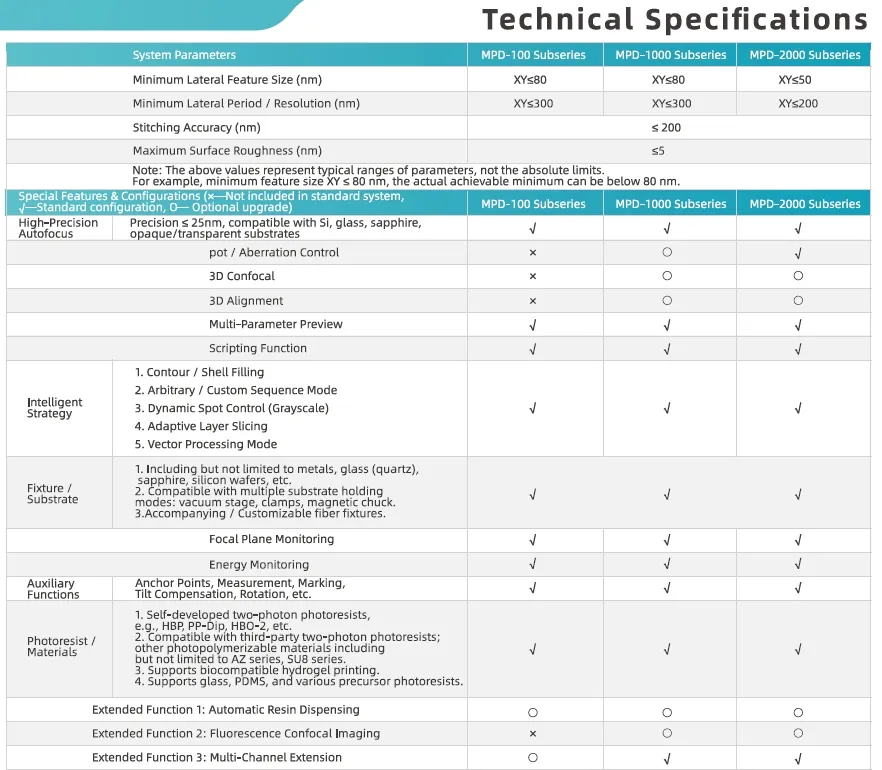
| Supported Printing Height | ≤10mm |
| Minimum Feature Width | ≤50nm (XY plane) and ≤300nm (Z-axis) |
| Maximum Scanning Speed | ≥100mm/s (1000mm/s@100x lens) |
| Stitching Accuracy | ≤100nm (XY plane) |
| Laser Parameters | Details |
| Central Wavelength | 515±5nm |
| Pulse Duration | ≤200fs |
| Repetition Rate | 80±5MHz |
| Installation Conditions | Details |
| Cleanroom Requirement | Class 1000 or above |
| Environmental Stability | 20±1ºC; ±0.1ºC stability |
| Ambient Lighting | Yellow Light |