1 / 5
| Parameter | Details |
|---|---|
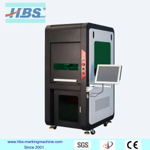
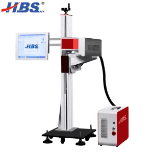
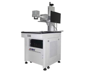
| Laser Wavelength | 532nm / 355nm / 1064nm |
| Cooling Method | Water Cooling / Air Cooling |
| Control System | Galvanometer + Control Card (Windows 7/10) |
| Supported File Formats | DXF, PLT |
| Power Supply | Single-Phase 220V, 4KW |
| Optional Features | QR Code (DM), Custom Marking Designs, FFU Filter |
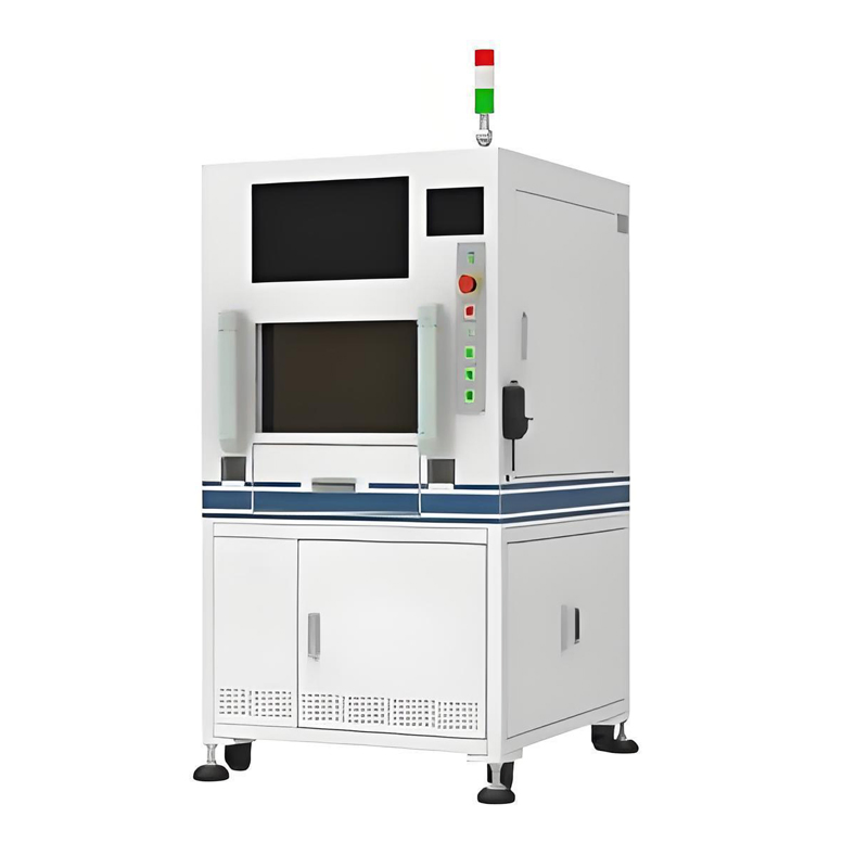
Temperature: 20-25°C
Humidity: 35-60% (no condensation)
Power: 220VAC, 50Hz, 32A
Compressed Air: ≥150L/min, 0.5-0.7MPa
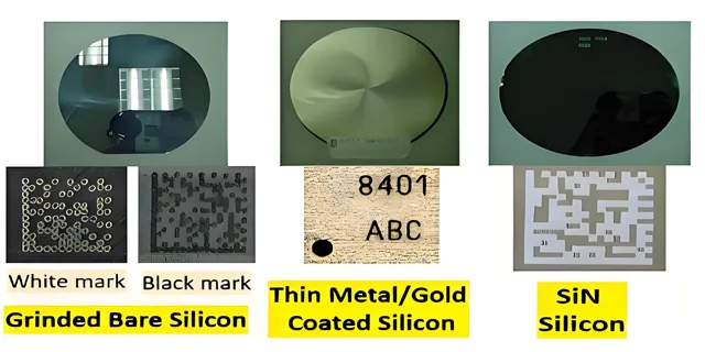
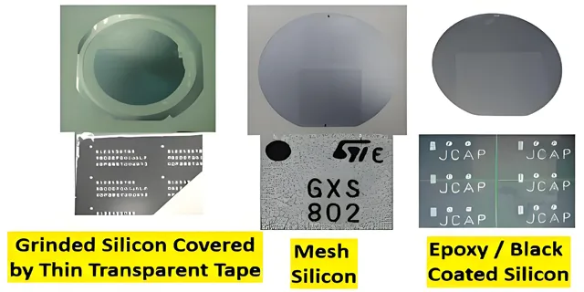
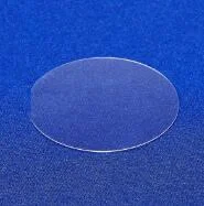
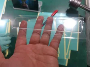
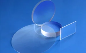
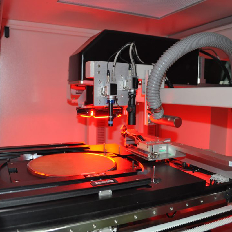
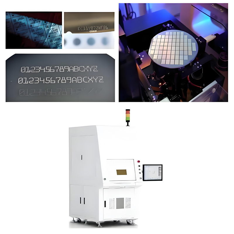
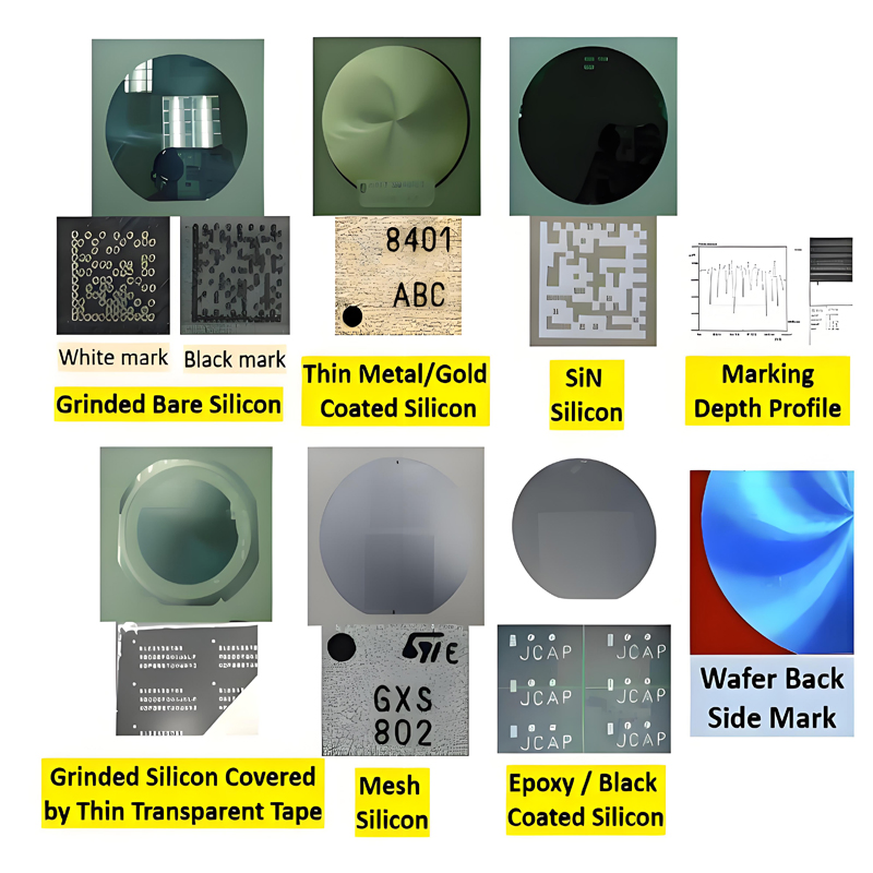
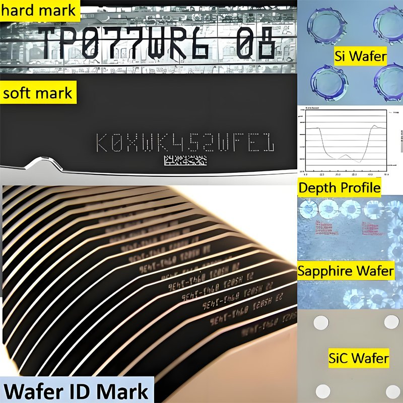
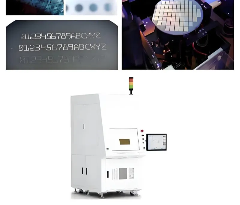
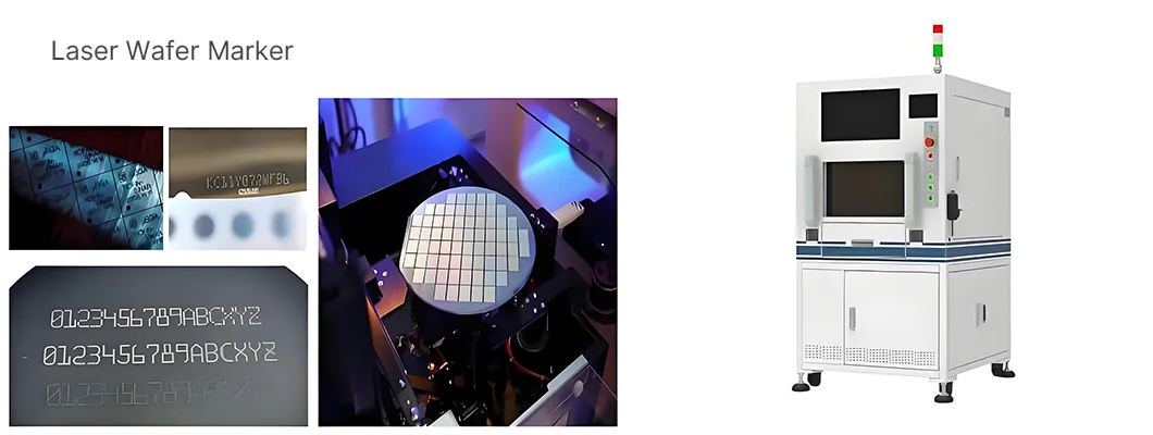
Equipped with specialized lasers for clear and durable wafer markings on Si, SiC, and GaN.
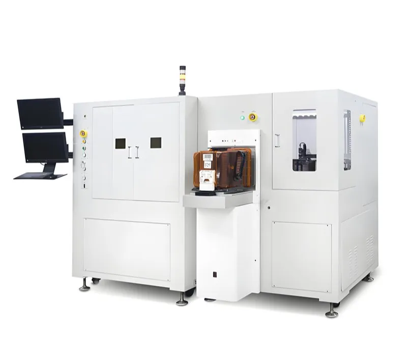
Dual-arm robotic system with ±0.1mm repeatability for seamless wafer loading/unloading.
Integrated 3-second center and angle detection for extremely accurate positioning.
Optional FFU (H14 filter, 99.997% efficiency) for ISO Class 2 environments.