


1 / 5
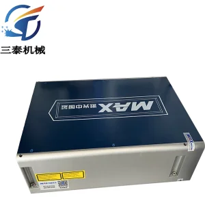
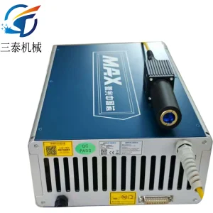
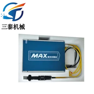
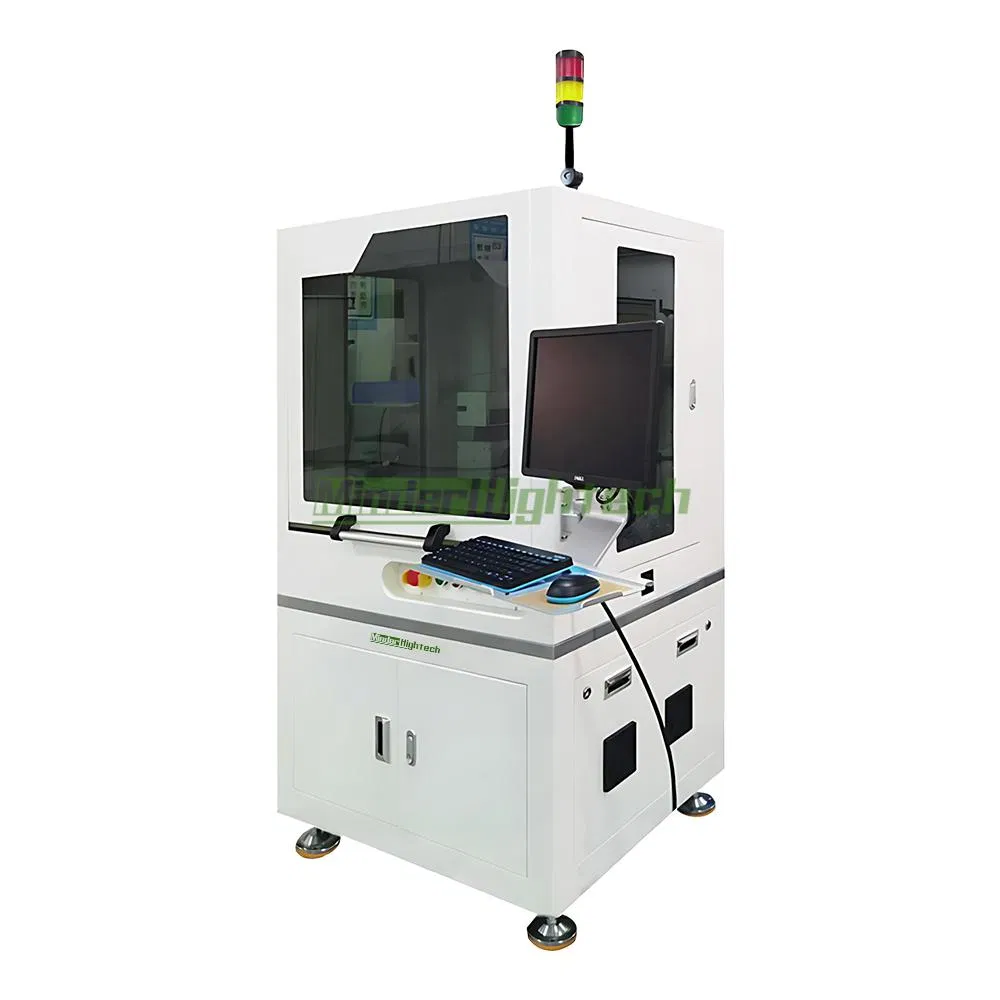
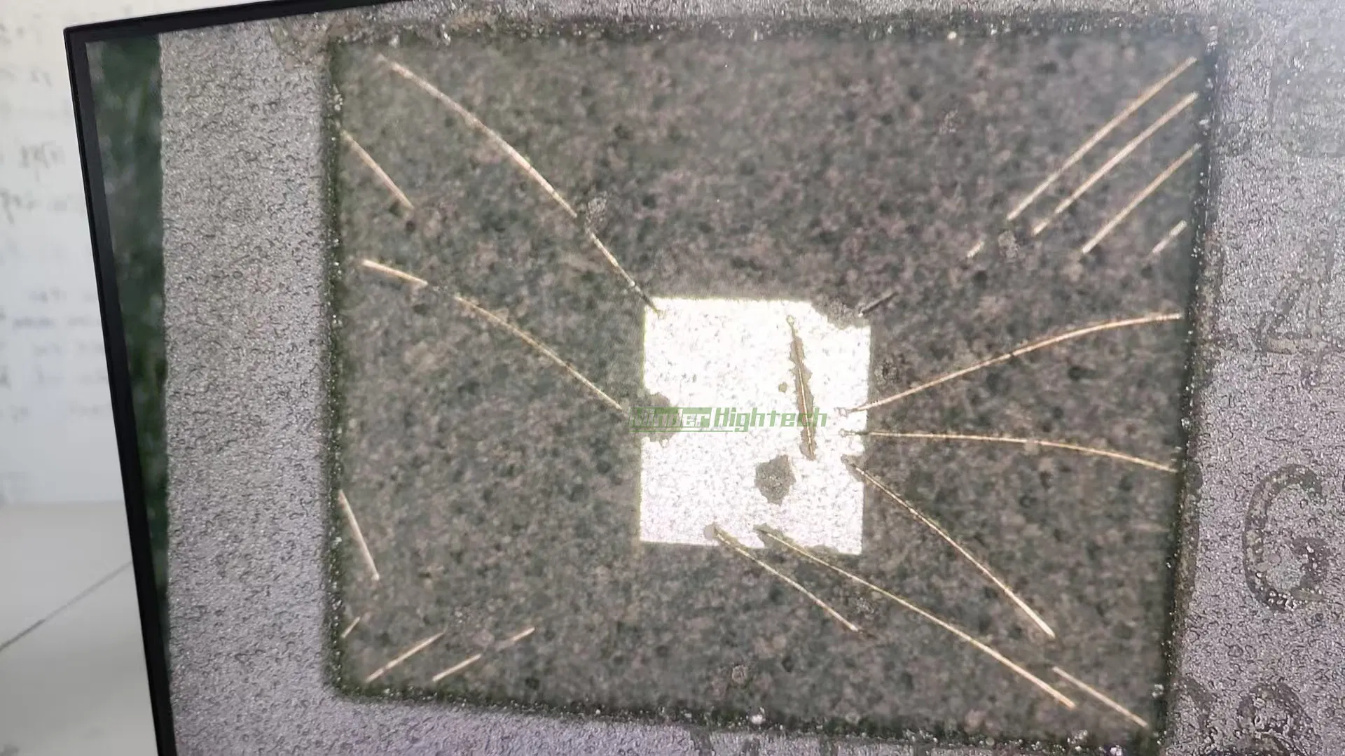
A high-precision laser decapsulation system designed for the efficient removal of epoxy and plastic molding materials from semiconductor devices.

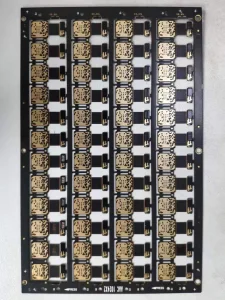
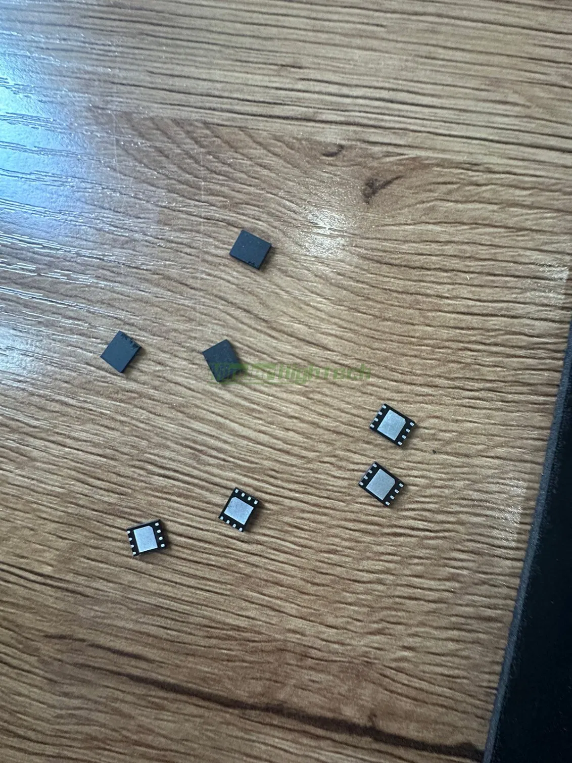
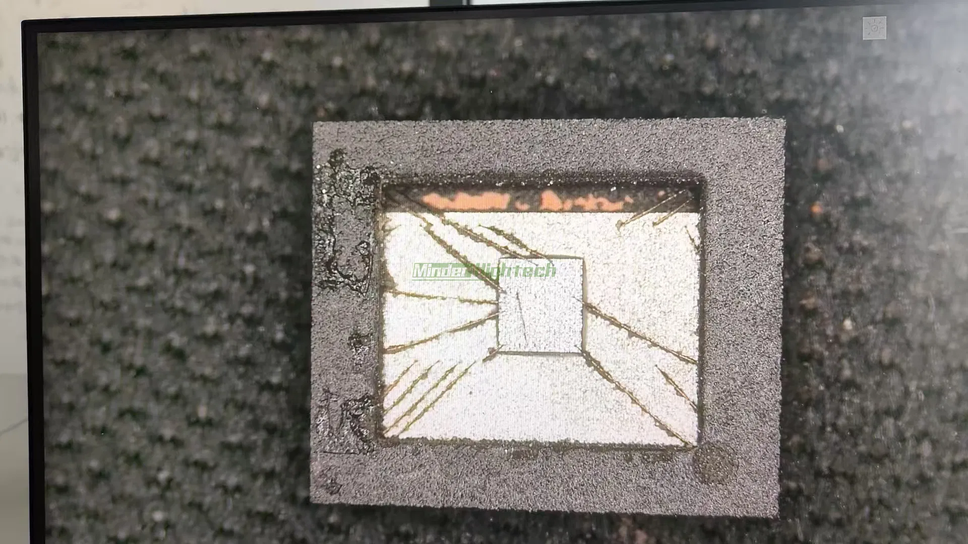
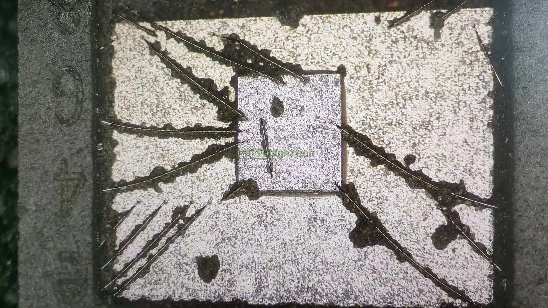
Primarily used for exposing the lead frame on the substrate of plastic-encapsulated semiconductor devices. It handles full-surface, targeted, or flat decapsulation, significantly reducing acid usage and chemical processing time.
Utilizes high-energy-density laser beams for micromachining. It interacts with matter to perform precise cleaning, engraving, and material removal on both metals and non-metals.
| Parameter | Details |
|---|---|
| Laser wavelength | MOPA 30W, 1064nm |
| Optical configuration | Focal length 160mm/110mm x 110mm |
| Opening Area | Min: 0.1mm x 0.1mm / Max: 300mm x 300mm |
| Opening depth | 0.01mm - 10mm (Resolution: 0.001mm) |
| Scanning speed | >8000mm/s |
| Positioning method | Visual recognition-assisted + CCD monitoring |
| Cleaning | Vacuum suction dust removal |
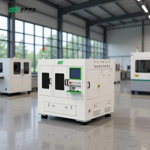
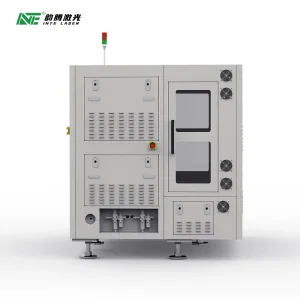
| Dimensions | 1150mm(L) * 1000mm(W) * 1750mm(H) |
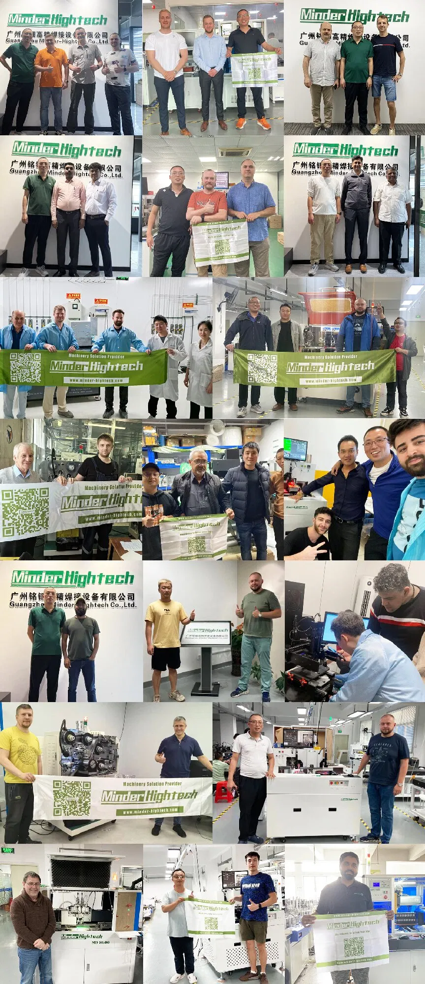
Since 2014, we have served as a professional sales and service representative in the Semiconductor and Electronic product industry equipment sector. We are committed to providing customers with superior, reliable, and one-stop solutions for machinery equipment.
Our products are utilized in major industrialized countries worldwide, helping clients improve efficiency, reduce operational costs, and enhance overall product quality.