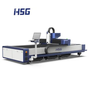
The global landscape for Custom Laser Services has shifted from simple engraving to complex, micro-scale industrial processing. As industries like semiconductors, aerospace, and medical devices demand higher precision, the role of manufacturers has evolved. Today, custom laser services represent a multi-billion dollar industry driven by the need for non-contact material removal, ultra-fine accuracy, and high-speed production cycles.
In the current industrial climate, businesses are no longer looking for "off-the-shelf" solutions. Instead, they require tailor-made systems capable of handling specific substrates such as Polyimide films, sapphire glass, and multi-layer PCBs. This demand for customization has led to the rise of specialized manufacturers who can integrate AI-driven CNC software with ultra-fast picosecond and femtosecond laser sources.
Cutting Accuracy
Global Industries Served
Efficiency Increase
Industrial Reliability
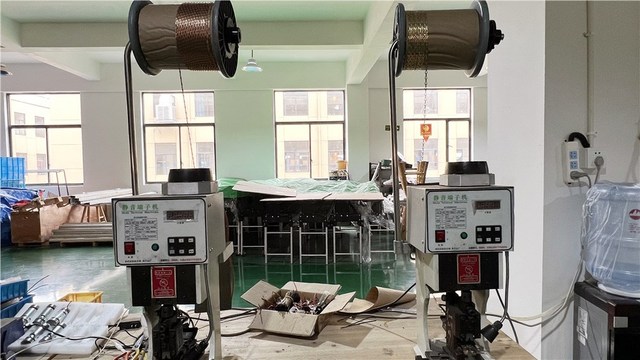
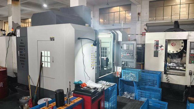
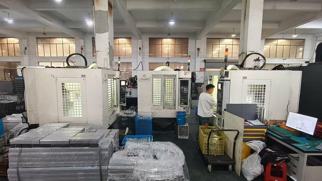
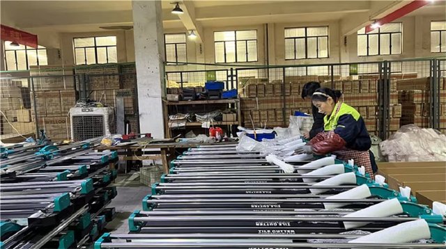
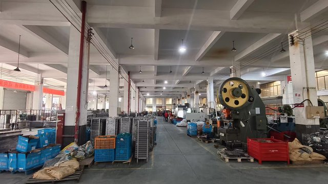
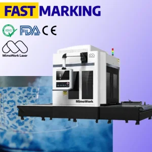
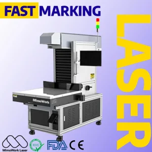
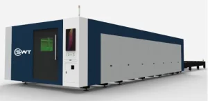
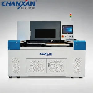
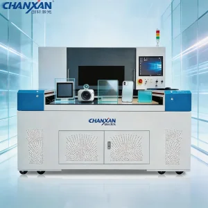
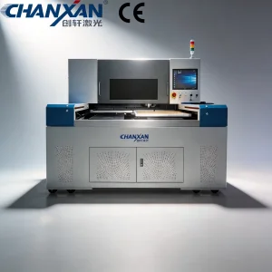
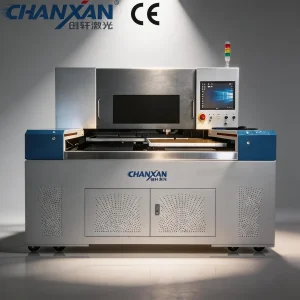
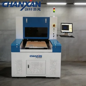
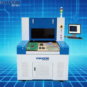
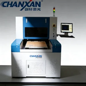
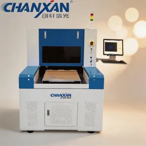
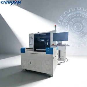
Hangzhou Focus Laser Co., Ltd. is a professional manufacturer specializing in advanced laser processing equipment for the electronics and display industries. The company focuses on the development and production of PCB laser cutting machines and glass laser cutting systems, delivering high-precision solutions for micro-electronics manufacturing and optical material processing.
Its technologies are widely applied in PCB depaneling, flexible circuit board processing, semiconductor packaging, and precision glass cutting for smartphones, display panels, and optical components. By integrating fiber laser technology, ultra-fine beam control, and intelligent CNC systems, Hangzhou Focus Laser ensures high cutting accuracy, smooth edges, and minimal thermal damage during processing.
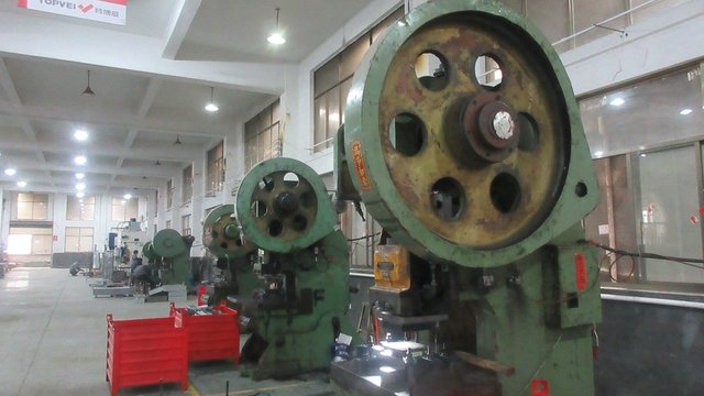
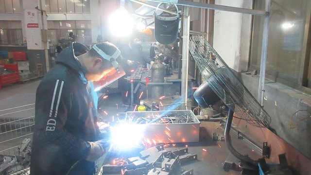
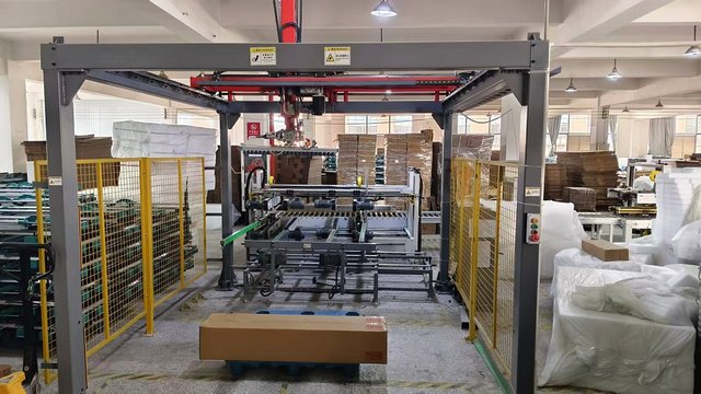
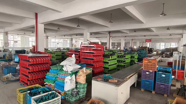
The company’s equipment is extensively used in industries such as consumer electronics, semiconductor manufacturing, automotive electronics, and smart display production. It supports both high-volume industrial production and customized precision machining requirements.
Hangzhou Focus Laser Co., Ltd. emphasizes innovation, reliability, and engineering excellence. With strong R&D capabilities and strict quality control standards, the company provides OEM and ODM services to meet global customer needs. Continuously advancing laser micro-processing technology, it aims to become a leading global supplier of precision laser solutions for PCB, glass, and advanced electronic manufacturing applications.
The transition from nanosecond to Picosecond and Femtosecond lasers is the biggest trend. These "cold processing" techniques prevent thermal deformation, essential for medical stents and flexible OLED screens.
Custom laser services now utilize AI vision systems for real-time alignment and defect detection, reducing waste and ensuring ±1μm accuracy across high-volume batches.
Laser technology is replacing chemical etching and traditional mechanical cutting, significantly reducing hazardous waste and energy consumption in the electronics supply chain.
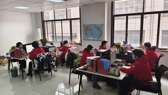
As a leading Chinese Laser Factory, we offer distinct advantages that go beyond cost-effectiveness. The integration of the entire supply chain allows us to respond to custom requests faster than European or North American competitors.
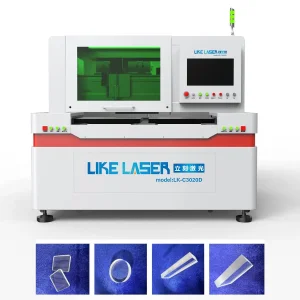
Understanding the application scenario is critical for Custom Laser Services. For example, in the 3C Display industry, glass cutting isn't just about separation; it's about "splitting" with micron-level precision to ensure the structural integrity of the smartphone screen. Our Integrated Glass Laser Cutting and Splitting Machines are designed specifically for these high-stakes environments.
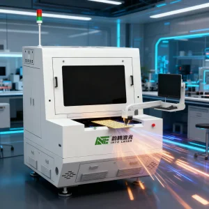
In the Semiconductor and MEMS sector, the challenge is handling ultra-thin wafers. Our Femtosecond Laser Cutting Machines utilize pulses so short that the material is vaporized before heat can conduct to adjacent areas, allowing for the processing of sensitive polyimide films and thin wafers without any carbonization or burrs.
For Flexible Printed Circuits (FPC), our UV Picosecond systems provide the ideal balance of speed and precision, ensuring that the complex conductive paths of modern smartphones and wearables remain intact during the depaneling process.