Explore our high-performance precision laser systems designed for modern electronics manufacturing.
The transition from mechanical routing to laser processing is reshaping the global SMT and PCB assembly industries.
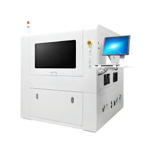
Globally, the demand for Laser Depaneling Equipment is surging as electronics become smaller and more complex. Traditional mechanical stress is no longer acceptable for high-density interconnect (HDI) boards. Laser technology offers a non-contact, stress-free solution that ensures zero damage to sensitive components.
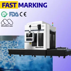
The industry is moving toward Ultrafast Lasers (Picosecond and Femtosecond) to achieve "cold processing." This trend is driven by the need for ultra-clean edges and minimal carbonization in flexible circuits (FPC) and rigid-flex boards used in 5G smartphones and wearable devices.
Major Tier-1 manufacturers in North America, Europe, and Southeast Asia are increasingly seeking integrated solutions that combine high precision with high-speed CNC systems. Key requirements include automated optical inspection (AOI) integration and compatibility with Industry 4.0 data standards.
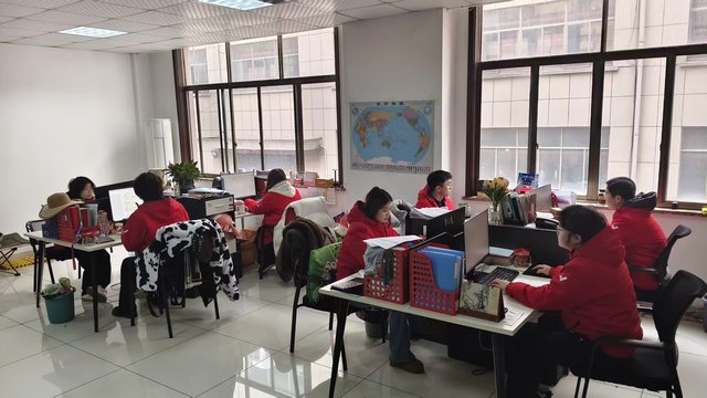
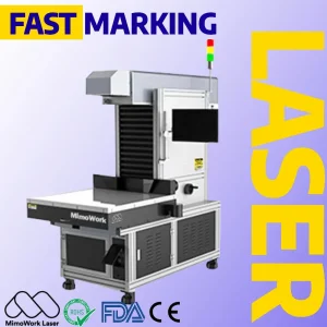
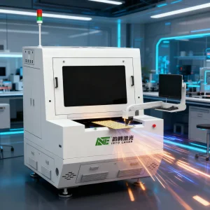
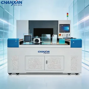
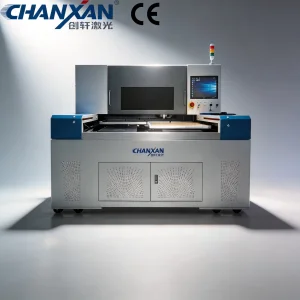
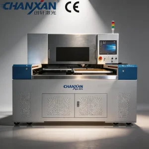
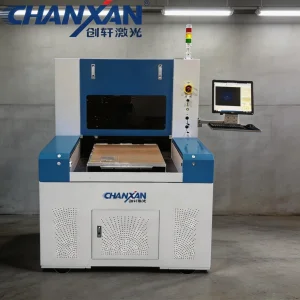
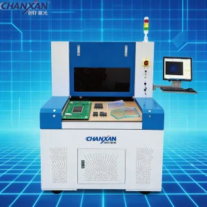
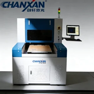
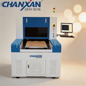
Hangzhou Focus Laser Co., Ltd. is a professional manufacturer specializing in advanced laser processing equipment for the electronics and display industries. The company focuses on the development and production of PCB laser cutting machines and glass laser cutting systems, delivering high-precision solutions for micro-electronics manufacturing and optical material processing.
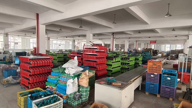
Its technologies are widely applied in PCB depaneling, flexible circuit board processing, semiconductor packaging, and precision glass cutting for smartphones, display panels, and optical components. By integrating fiber laser technology, ultra-fine beam control, and intelligent CNC systems, Hangzhou Focus Laser ensures high cutting accuracy, smooth edges, and minimal thermal damage during processing.
The company supports both high-volume industrial production and customized precision machining requirements, emphasizing innovation, reliability, and engineering excellence.
Our equipment is engineered to solve specific regional manufacturing challenges.
Used extensively in China and Vietnam's assembly hubs for cutting mobile phone display panels, camera modules, and FPC finger-print sensors.
Crucial for European and American automotive suppliers in manufacturing ADAS sensor PCBs and high-voltage power electronics that require extreme durability.
Applied in the production of biocompatible circuits and micro-fluidic chips, where precision and cleanliness are non-negotiable parameters.
Combining world-class R&D with a robust supply chain to deliver unmatched value.
Strong internal R&D ensures we stay at the forefront of UV and Femtosecond laser technology integration.
Localized supply chains allow us to offer factory-direct prices without compromising on premium component quality.
We provide tailored solutions, from custom CNC software to specialized jig designs for unique PCB geometries.
Strict adherence to international standards ensures every machine shipped is reliable for 24/7 industrial use.
Highly specialized equipment for 3C display panels and semiconductor materials.
Choosing the right Laser Depaneling Equipment Manufacturer is critical for maintaining high yields in modern electronics manufacturing. As components move closer to the edge of the PCB, mechanical stress from traditional routers or dies can cause invisible micro-cracks in ceramic capacitors and solder joints.
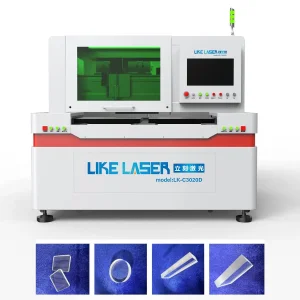
Our 355nm UV Laser systems utilize "cold processing," where the laser's high-energy photons directly break the molecular bonds of the material. This results in an extremely narrow kerf width (typically <20μm) and virtually no heat-affected zone (HAZ). This is essential for COB substrates and FPC processing, where thermal expansion can ruin delicate circuit traces.
For the most demanding applications, such as MEMS device cutting and thin wafer dicing, our Femtosecond Laser Cutting Machines provide ±1μm accuracy. By delivering pulses in the quadrillionth of a second, the laser evaporates material before heat can transfer to the surrounding area, enabling the machining of incredibly brittle materials like glass and sapphire without fracturing.