With decades of focus on laser micro-processing, we understand the intricate needs of semiconductor and electronics manufacturing.
Integrating Picosecond, Femtosecond, and UV laser technologies with intelligent CNC and fiber beam control for sub-micron accuracy.
A trusted partner for Fortune 500 companies, providing certified equipment that meets stringent international safety and quality standards.
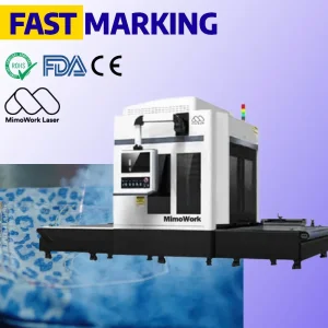
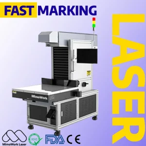
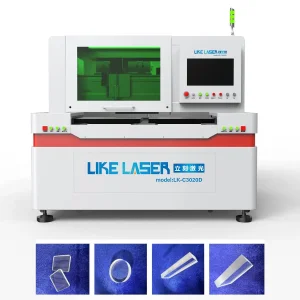
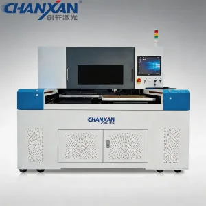
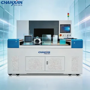
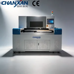
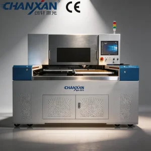
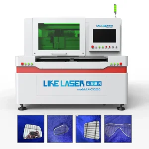
Hangzhou Focus Laser Co., Ltd. is a professional manufacturer specializing in advanced laser processing equipment for the electronics and display industries. The company focuses on the development and production of PCB laser cutting machines and glass laser cutting systems, delivering high-precision solutions for micro-electronics manufacturing and optical material processing.
Its technologies are widely applied in PCB depaneling, flexible circuit board processing, semiconductor packaging, and precision glass cutting for smartphones, display panels, and optical components. By integrating fiber laser technology, ultra-fine beam control, and intelligent CNC systems, Hangzhou Focus Laser ensures high cutting accuracy, smooth edges, and minimal thermal damage during processing.
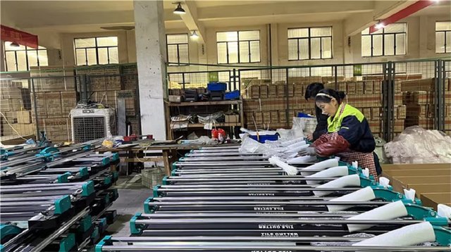
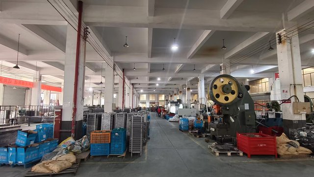
The company’s equipment is extensively used in industries such as consumer electronics, semiconductor manufacturing, automotive electronics, and smart display production. It supports both high-volume industrial production and customized precision machining requirements.
Hangzhou Focus Laser Co., Ltd. emphasizes innovation, reliability, and engineering excellence. With strong R&D capabilities and strict quality control standards, the company provides OEM and ODM services to meet global customer needs. Continuously advancing laser micro-processing technology, it aims to become a leading global supplier of precision laser solutions for PCB, glass, and advanced electronic manufacturing applications.
The global industrial sector is undergoing a massive shift toward Industry 4.0, where precision and automation are no longer optional but essential. Advanced laser automation has emerged as the cornerstone of this transition. From the Silicon Valley tech giants to the massive manufacturing hubs in Southeast Asia and Europe, the demand for non-contact, high-speed, and ultra-precise processing is skyrocketing.
Today, the laser automation market is valued at over 20 billion USD. The rise of 5G, New Energy Vehicles (NEVs), and foldable display technologies has created a "precision bottleneck" that traditional mechanical cutting cannot solve. Laser systems, specifically Picosecond and UV lasers, provide the necessary cold-processing capabilities to handle sensitive materials like ultra-thin glass (UTG) and multilayer PCBs without thermal deformation.
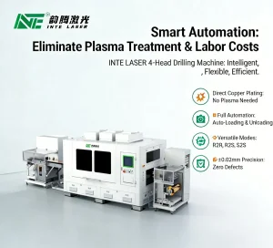
The trend is moving toward "Intelligent Ultra-fast Processing". This includes the integration of AI-driven vision systems for real-time defect detection and automatic path correction. Furthermore, multi-head laser systems are becoming the standard for high-throughput manufacturing, allowing factories to double or quadruple production output without increasing their floor footprint.
Understanding the specific needs of different regional markets is what sets Hangzhou Focus Laser apart as a global OEM/ODM leader.
Focus on Aerospace and Medical Device manufacturing. Demand for high-compliance, traceable laser marking and cutting of biocompatible materials.
Heavy emphasis on Automotive Electronics. Our systems assist in the production of EV battery sensors and high-performance dashboard displays.
The global hub for Consumer Electronics assembly. We provide high-volume PCB depaneling and glass splitting machines for smartphone assembly lines.
As a leading Chinese Manufacturer, Hangzhou Focus Laser offers a unique "Triple Advantage":
Used in the precision splitting of tempered glass and OLED screens. Our Picosecond technology ensures zero chipping and edge strength that meets flagship smartphone standards.
Ideal for Flexible Printed Circuits used in wearable tech. Laser cutting eliminates mechanical stress, preventing delicate micro-solder joint fractures.
Precision drilling and marking for engine sensors and autonomous driving LIDAR components, ensuring durability under extreme conditions.
Wafer dicing and marking with ultra-fine beams, facilitating the miniaturization of modern microchips.
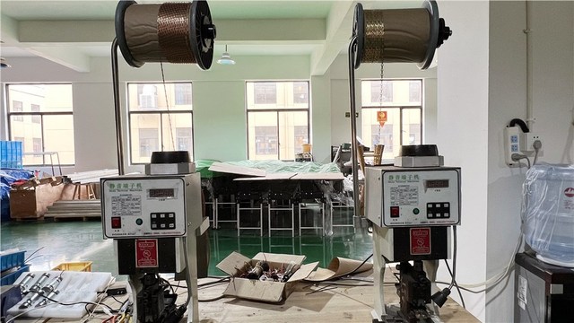
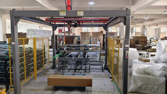
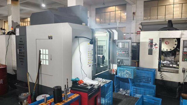
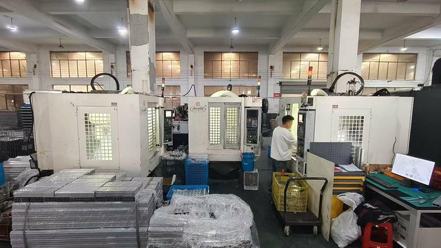
As an industry-leading OEM/ODM partner, our facility is equipped with state-of-the-art testing laboratories to ensure every machine delivered meets global industrial benchmarks.

Our machines use high-resolution CCD cameras to automatically recognize fiducial marks on PCBs or glass panels, ensuring alignment precision within ±5μm.
Whether your application requires 1064nm (Fiber), 532nm (Green), or 355nm (UV), our modular laser sources are interchangeable for maximum flexibility.
Fully compatible with SMEMA standards, allowing our laser systems to integrate seamlessly into your existing SMT or assembly lines with robotic loading/unloading.