High-reliability optical sub-assemblies, localized CNC platforms, and laser marking hardware tailored for extreme duty cycles.

A Premier Manufacturer Specializing in Advanced Laser Processing Systems for the Electronics, Display, and Micro-semiconductor Industries.
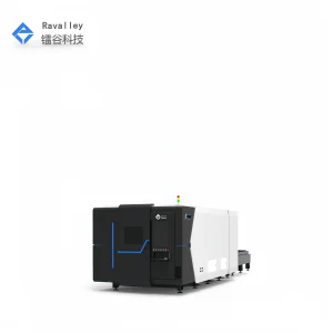
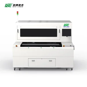
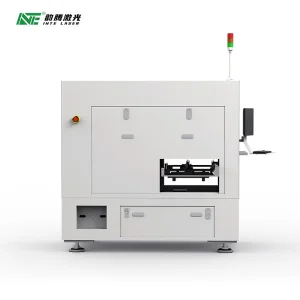
At Hangzhou Focus Laser Co., Ltd., we sit at the intersection of optoelectronic engineering and industrial-grade software control. Our operational core lies in developing and manufacturing next-generation PCB laser cutting machines and glass laser cutting systems. By providing high-precision solutions specifically calibrated for micro-electronics fabrication, we assist global OEMs in navigating the challenges of component miniaturization and advanced material integration.
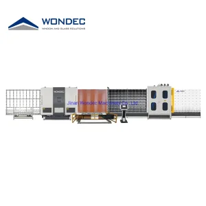
Our technologies find extensive application across fields such as flexible circuit board (FPC) processing, semiconductor packaging, and precision glass profiling for consumer smart devices. By utilizing advanced fiber laser modules, ultra-fine galvo-beam control, and proprietary intelligent CNC architectures, we guarantee high-precision edges, minimal Heat Affected Zones (HAZ), and structural integrity on even the most delicate substrates.
Decoding the technical shift from mechanical abrasive processing to cold-ablation laser technologies.
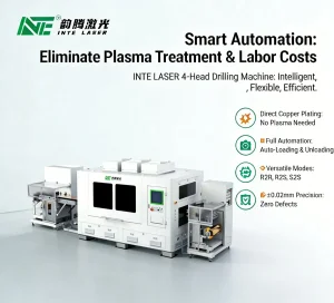
Traditional routing machines inflict physical stress on delicate SMD components. Our UV and fiber laser solutions execute non-contact cutting, eliminating board warp, dust emissions, and mechanical tool wear, raising yields in high-density HDI production.
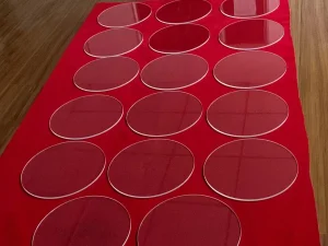
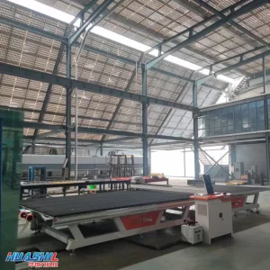
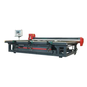
Processing chemically strengthened aluminosilicate glass or sapphire panels requires precision parameters to avoid micro-cracking. Our high-power CNC glass cutting lines deliver micro-meter edge quality with near-zero chipping profiles.
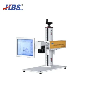
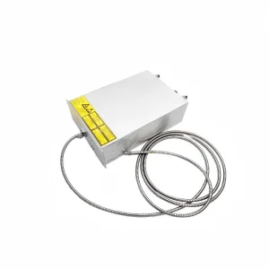
In modern industrial workflows, traceability is mandatory. Our UV laser marking platforms provide durable, high-contrast, permanent micro-codes on reflective, composite, or brittle materials without compromising the structural integrity of the substrate.
Across Europe, North America, and high-tech manufacturing corridors in Asia, the adoption of sub-micron precision is accelerating. Historically, mechanical diamond scribing was the baseline for display panel cutting. However, as consumers demand thinner bezels, curved profiles, and ultra-thin flexible screens, mechanical methods cannot scale. Laser cold-ablation technology—especially utilizing 355nm and 405nm ultraviolet spectrum modules—solves this by breaking chemical bonds directly rather than melting materials thermally. Hangzhou Focus Laser helps bridge this gap by delivering systems that lower high technology capital expenditure barriers, maintaining robust throughput speeds while achieving world-class precision tolerances.
Understanding the physics of high-power fiber-coupling and UV laser processing.
In the domain of PCB lithography, direct imaging, and high-precision curing, the wavelength selection is critical. The 405nm UV spectrum offers an optimal balance between photo-initiator absorption rates and glass fiber transmission efficiency. By utilizing high-power fiber-coupled configurations (up to 100W), optical energy is compressed into narrow-core fibers (typically 100µm to 200µm). This delivery mechanism ensures a highly circular beam profile (low M² factor), enabling consistent energy delivery at the work surface.
For glass and sapphire profiling, short-pulse UV lasers emit photons with energy high enough to trigger photo-dissociation. Because this action bypasses thermal phase transitions, it minimizes the creation of micro-fractures, which could otherwise weaken the tempered structure of mobile device screens or industrial viewing windows.
Hardware power is only half the equation. The precision of a laser cutting or marking machine relies on its CNC controller and scan-head synchronization. By combining high-speed digital galvos with linear-motor-driven XY stages, our equipment provides on-the-fly marking and high-speed vector cutting. Real-time feedback loops correct for optical distortion across the entire f-theta scan field, ensuring that a micro-drill hole or marked data matrix on the corner of a panel maintains the exact dimensional parameters as one in the center.
When selecting a laser supplier, engineers must evaluate critical parameters. The table below represents the core design targets of Hangzhou Focus Laser's equipment line:
| System Parameter | Standard Specification | Performance Target |
|---|---|---|
| Wavelength Availability | 355nm, 405nm, 1064nm | Cold & Thermal Ablation |
| Positioning Accuracy | ±0.005 mm | High-yield micro-electronics |
| Max Processing Speed | Up to 800 mm/s (glass) | High-volume industrial lines |
| Heat Affected Zone (HAZ) | < 15 µm | Negligible mechanical stress |
| MTBF of Diode System | > 20,000 Hours | Continuous 24/7 factory operation |
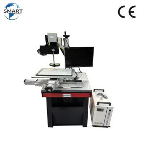
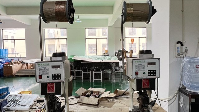
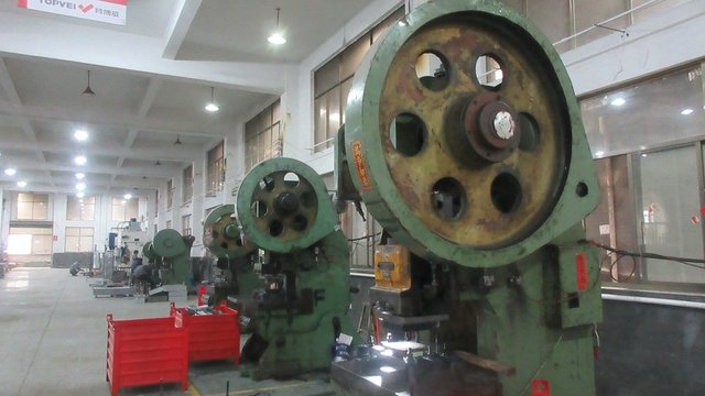
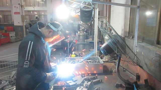
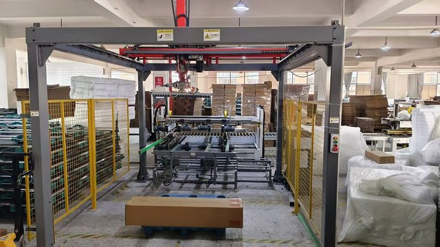
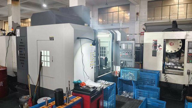
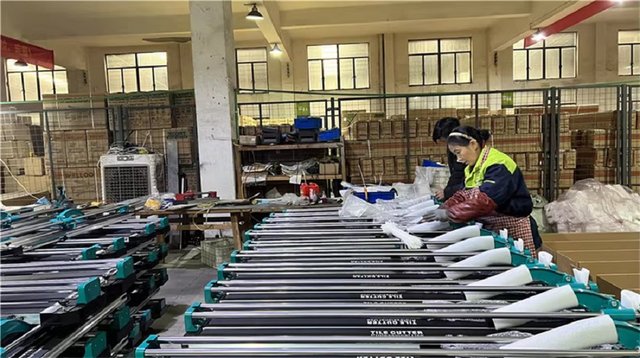
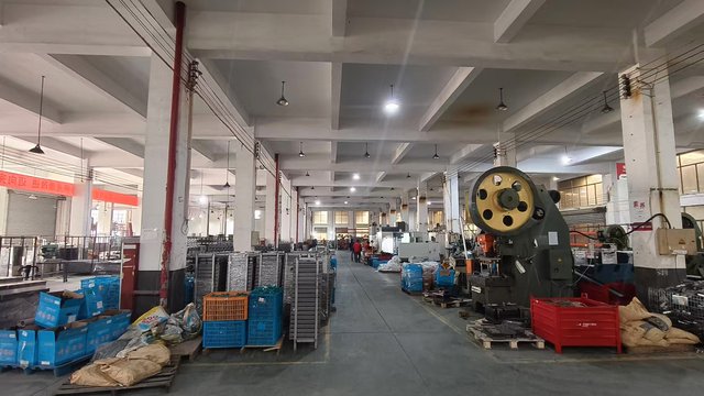
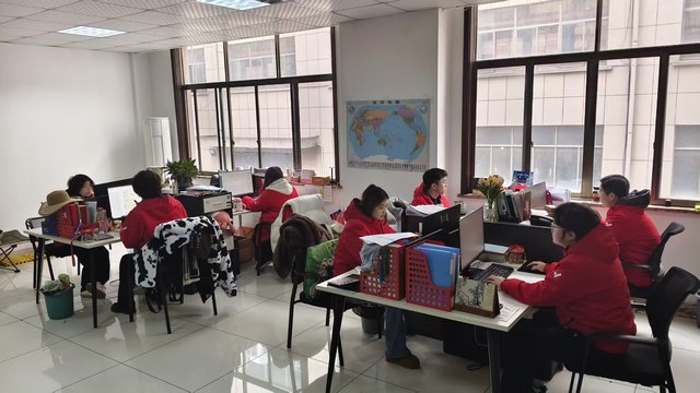
Behind-the-scenes view of our design, assembly, quality control, and testing environments.
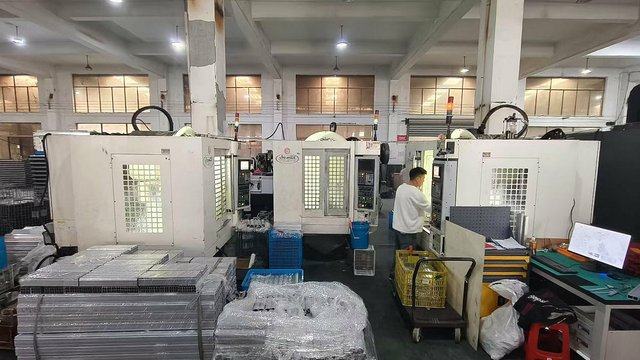
Building reliable operational partnerships through standardized engineering audits.
Deploying machinery into international facilities requires rigorous compliance. Hangzhou Focus Laser systems are engineered to meet CE directives, RoHS environmental guidelines, and FDA CDRH laser safety standards (Class I integrated workstations, Class IV subsystems). We employ high-density optical enclosure systems, dual interlocks, and specialized exhaust integrations to control micro-particulates generated during processing.
To reduce installation lead times, we perform full-scale Factory Acceptance Testing (FAT) using customer-supplied materials. Our diagnostics run on high-resolution beam profiling equipment, measuring laser power stability, spot size roundness, and spatial path deviations. All calibration data is generated in comprehensive PDF logs and is verifiable via live remote video audits prior to overseas shipment.
Our localized support network ensures prompt assistance in key manufacturing corridors. We provide standard installation and training services including:
The future of ultra-short pulse (USP) lasers, AI-driven process optimization, and smart factory integration.
As microchip designs shrink, even the small heat-affected zones of nanosecond lasers can become a factor. Our research team is designing compact picosecond and femtosecond fiber-coupled laser sources. By delivering gigawatt-level peak power in short pulse bursts, these lasers vaporize material before heat can conduct into neighboring structures.
Future CNC platforms will feature closed-loop visual systems powered by edge computing. By integrating high-resolution digital cameras, our systems can detect substrate warping, micro-cracks, or alignment drift, dynamically adjusting the laser power, focal position, and marking path in real time to prevent defects.
To align with Smart Factory goals, our entire CNC glass cutting and marking product line is adopting the OPC Unified Architecture (OPC-UA). This enables manufacturing executives to monitor laser tube temperatures, gas levels, scan speeds, and cycle efficiency metrics through centralized MES dashboards.
Authoritative explanations regarding laser safety, beam selection, and system installation.
405nm UV lasers provide a shorter wavelength compared to near-infrared (1064nm) platforms. Short wavelengths feature a much smaller focal spot size, allowing for high-precision micro-machining. Additionally, UV photons break chemical bonds directly (cold ablation) rather than relying on high heat to melt the target material. This virtually eliminates the Heat Affected Zone (HAZ), preventing charring or structural warping in delicate substrates like PCB materials, flexible polyimides, and glass.
Yes. Our CNC glass cutting systems utilize optimized short-pulse optical paths and proprietary CNC motion control to profile chemically strengthened display panels, sapphire windows, and ultra-thin glass cover sheets. By tuning pulse frequency and step speeds, the systems control edge stress profiles to prevent cracking along cut paths.
We provide localized engineering support through installation documentation, pre-delivery Factory Acceptance Testing (FAT) logs, and remote video audits. Our international distribution partners also maintain stocks of critical components to ensure replacement optics or control modules are shipped promptly when needed.
UV marking systems are highly versatile due to their non-thermal chemical marking process. They excel at marking plastics (such as HDPE, PVC, and ABS), optical glass, high-purity quartz, medical-grade silicones, and ceramic materials. The result is a high-contrast mark that does not damage the surrounding material, making it ideal for medical, aerospace, and semiconductor packaging industries.
Yes. Our R&D team specializes in designing custom laser modules, fiber-coupling optics, and specific CNC gantry sizes. We work directly with your engineering team to integrate our laser systems into existing production lines or create custom workstations tailored to your factory layout and material flow requirements.
High-capacity production tools, specialty components, and environmentally sound PV reclamation units.