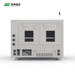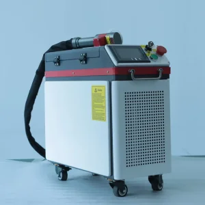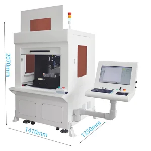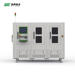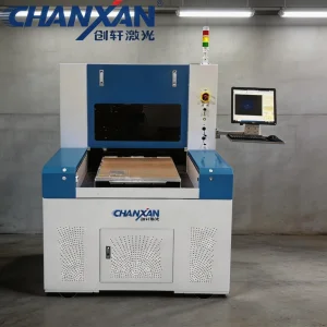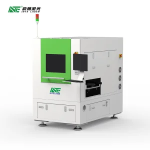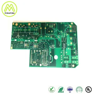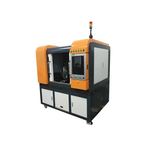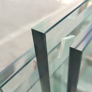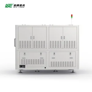
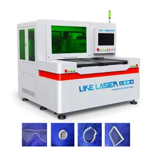
Hangzhou Focus Laser Co., Ltd. is a professional manufacturer specializing in advanced laser processing equipment for the electronics and display industries. The company focuses on the development and production of PCB laser cutting machines and glass laser cutting systems, delivering high-precision solutions for micro-electronics manufacturing and optical material processing.
Its technologies are widely applied in PCB depaneling, flexible circuit board processing, semiconductor packaging, and precision glass cutting for smartphones, display panels, and optical components. By integrating fiber laser technology, ultra-fine beam control, and intelligent CNC systems, Hangzhou Focus Laser ensures high cutting accuracy, smooth edges, and minimal thermal damage during processing.
The company’s equipment is extensively used in industries such as consumer electronics, semiconductor manufacturing, automotive electronics, and smart display production. It supports both high-volume industrial production and customized precision machining requirements.
Hangzhou Focus Laser Co., Ltd. emphasizes innovation, reliability, and engineering excellence. With strong R&D capabilities and strict quality control standards, the company provides OEM and ODM services to meet global customer needs. Continuously advancing laser micro-processing technology, it aims to become a leading global supplier of precision laser solutions for PCB, glass, and advanced electronic manufacturing applications.
The modern precision processing landscape is rapidly transitioning from nanosecond lasers to ultra-short pulse regimes, notably femtosecond and picosecond laser technologies. This transition is motivated by the physical mechanisms of material ablation. Unlike continuous or long-pulsed lasers that melt materials through photothermal effects (often causing micro-cracking, heat-affected zones, and burrs), USP lasers deliver energy within durations shorter than the thermal diffusion time of the lattice. This process, known as "cold ablation," results in sub-micron precision, completely clean margins, and pristine structural integrity. It is especially critical when processing sensitive substrates such as flexible PCBs (FPC) and high-density packaging layers.
Static CNC positioning is no longer sufficient for complex modern geometries. Today's manufacturing systems integrate 6-axis articulated arms with multi-spectral machine vision systems. Real-time path correction algorithms analyze workpiece position, thermal distortion, and structural tolerances at a frequency of over 10 kHz. This high-frequency feedback loop allows the laser head to maintain a constant focal depth and incident angle, even across complex 3D curved surfaces. This adaptive tracking capability is essential for operations like high-speed automobile structural component cutting and display glass edge profiling.
To optimize operational expenditure (OpEx), factory floors are increasingly seeking hybrid platforms that combine multiple production stages into a single robotic cell. Typical configurations integrate laser cutting with surface activation, inline cleaning (removing ablation residues via high-frequency pulse cleaning), and 3D optical metrology. This consolidation minimizes material handling times, mitigates contamination risks, and reduces the physical footprint of the factory floor.
We design and engineer robotic laser systems to meet the unique challenges of today's core industries. By using advanced laser wavelengths (ranging from ultraviolet to infrared) and combining them with mechanical architectures, we provide turnkey solutions that improve yield rates and reduce cycle times.
As semiconductor components continue to shrink, traditional mechanical dicing techniques face limits. For example, wide-bandgap semiconductors like Silicon Carbide (SiC) and Gallium Nitride (GaN) are very hard and brittle, which can lead to micro-cracks and chipping during mechanical sawing. Our green and ultraviolet laser dicing systems use high peak power and short pulse widths to cut wafers with minimal kerf width. This process reduces heat-affected zones and improves the count of good dies per wafer.
Modern smartphones and wearable devices rely heavily on curved, ultra-thin, and chemically strengthened glasses. Traditional mechanical grinding introduces edge stresses that lower the material's overall mechanical strength. Our ultra-thin glass laser cutting systems use localized thermal shock or direct ablation to produce clean, stress-free edges. This eliminates the need for post-cut grinding, reducing manufacturing complexity and improving throughput.
Modern electronic devices pack more functionality into smaller form factors, driving the need for flexible PCBs. However, cutting materials like polyimide, copper foil, and adhesives without causing charring or delamination is difficult. Our picosecond UV laser systems use cold-cutting processes to cut FPCs cleanly. This minimizes carbonization, keeps the copper layers intact, and yields neat, functional components ready for assembly.
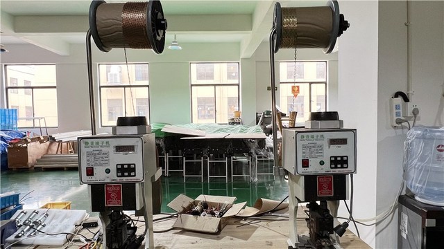
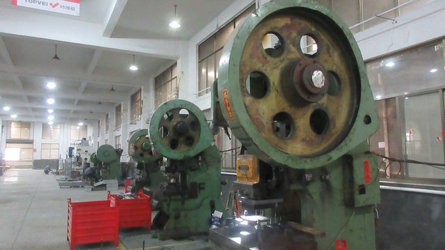
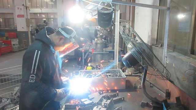
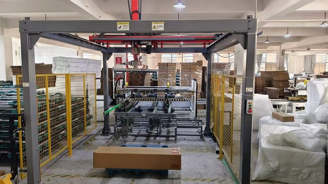
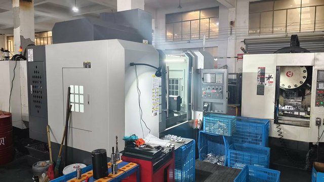
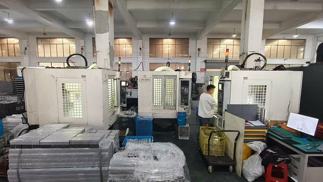
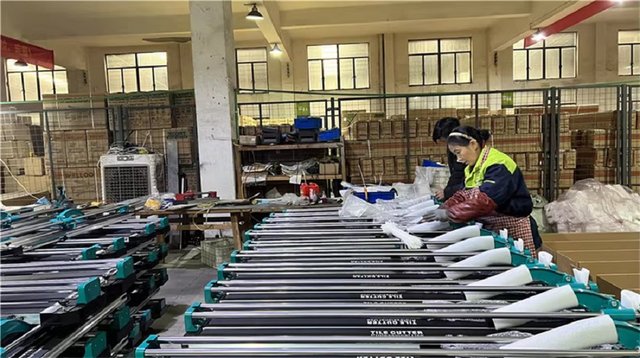
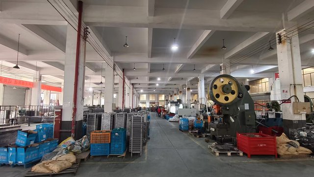
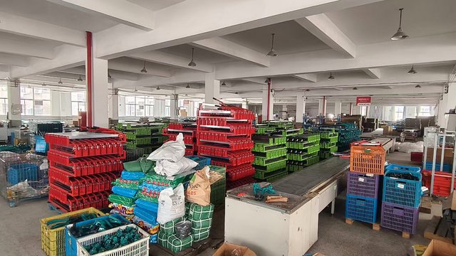
Our manufacturing facilities integrate cleanroom assembly bays, optical alignment stations, and stress-testing chambers. We control every stage of production—from the raw frame welding and robotic arm calibration to the final alignment of the optical path—to ensure consistency across all production runs.
To help our partners maintain a competitive edge, we focus our long-term R&D on emerging industry requirements. Our technical roadmap highlights three key areas:
 Focus Laser