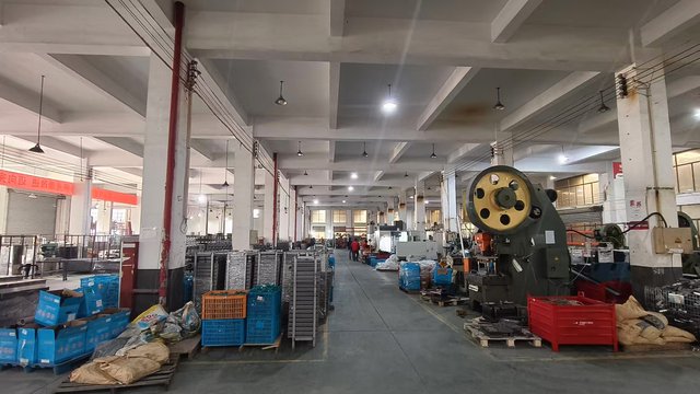
As the global semiconductor industry pivots towards Heterogeneous Integration and Advanced Packaging, China has emerged not just as a manufacturing hub, but as a primary innovator in precision backend solutions. The "Top China Semiconductor Packaging Solutions" are no longer defined by low-cost labor, but by state-of-the-art laser micro-machining, femtosecond technology, and automated inspection systems.
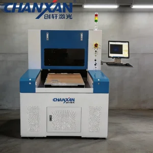
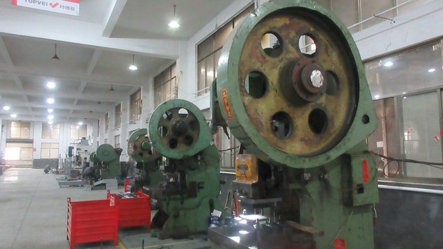
Leveraging decades of industrial laser expertise, Hangzhou Focus Laser Co., Ltd. exemplifies the transition from standard PCB depaneling to high-precision semiconductor substrate processing.
Deep specialization in UV, Fiber, and Femtosecond laser sources allows for "Cold Processing," minimizing Thermal Affected Zones (TAZ) in sensitive wafer-level packaging.
Compliance with ISO 9001 and CE certifications ensures that equipment meets the rigorous reliability standards of Tier-1 electronics manufacturers and OSATs.
The global semiconductor packaging market is projected to reach over $90 billion by 2028, driven by the explosive growth of Artificial Intelligence (AI), High-Performance Computing (HPC), and 5G telecommunications. In this landscape, the role of precision laser cutting has become critical. Traditional mechanical dicing methods are hitting their physical limits as wafers become thinner and materials more brittle (such as Silicon Carbide and Sapphire).
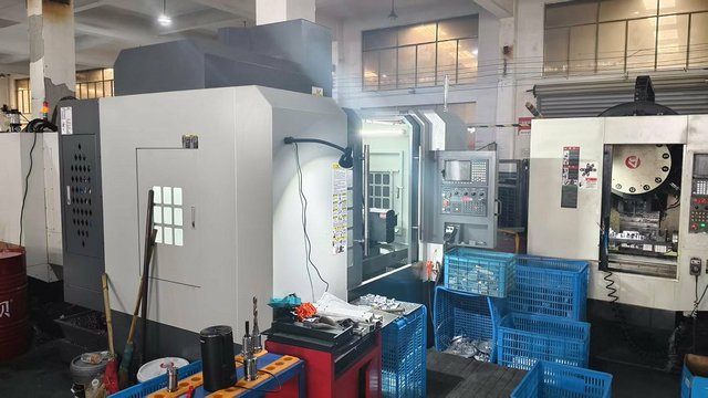
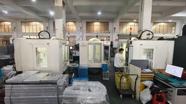
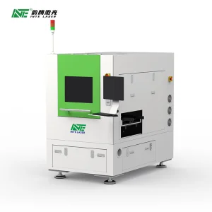
China's packaging solutions providers are integrating AI-driven CNC systems to achieve micron-level accuracy. By utilizing systems like the Fsd Crystal Materials Femtosecond Laser, manufacturers can now process complex gratings and optical components that were previously impossible to manufacture at scale. This technological leap addresses the global demand for Chiplets and 2.5D/3D packaging architectures, where vertical interconnects require flawless via-drilling and substrate separation.
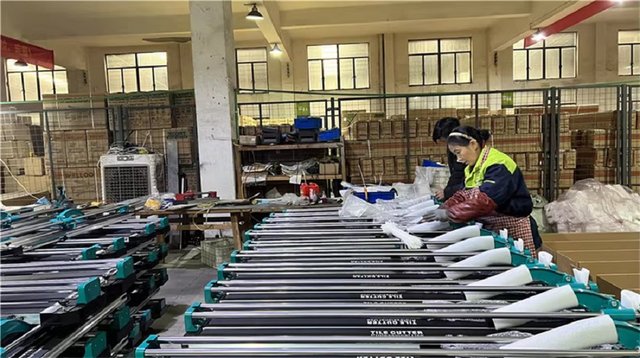
Current focus on PCB laser cutting and MEMS device fabrication. Utilizing ultra-fine beam control to support flexible circuit boards and smartphone display panels.
Expanding into Sapphire Tube processing, Plasma Chambers, and ceramic substrate machining. Essential for the next generation of power semiconductors (SiC/GaN).
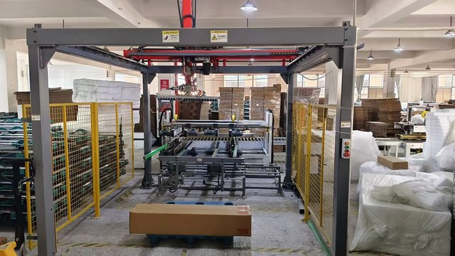
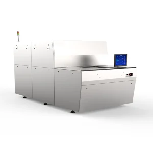
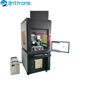
Development of autonomous laser splitting machines (like the 30W Fully Automatic series) with real-time AOI (Automated Optical Inspection) for zero-defect manufacturing.
Hangzhou Focus Laser Co., Ltd. is at the forefront of this roadmap. By integrating fiber laser technology and intelligent CNC systems, they ensure minimal thermal damage—a vital requirement for Advanced Packaging (AP) where heat can degrade the integrity of multi-stacked dies.
For international buyers, sourcing from China requires more than just high-spec hardware; it requires Reliability (R). Our solutions include:
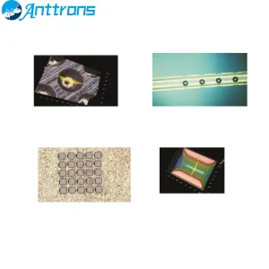
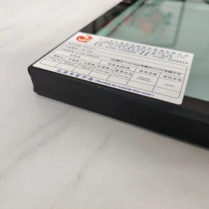
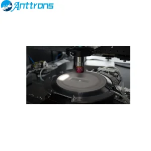
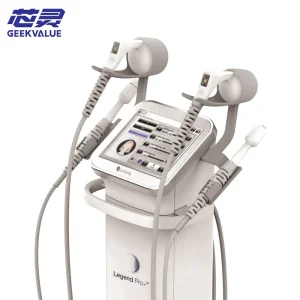
In the semiconductor world, "Interposers" require thousands of micro-vias. The Precision Microhole Machining System featured in our lineup is designed for efficient production processes. Unlike traditional drilling, laser micro-machining prevents micro-cracks in glass and ceramic substrates, which is essential for High-Frequency 6G applications and Medical Aesthetic Solutions (e.g., Lumenis Legend PRO+ platform components).
Laser machining offers a "non-contact" process, which eliminates mechanical stress on fragile semiconductor materials. This results in significantly higher yields, especially for Thin-Wafer processing and complex geometries.
By combining over a decade of Experience in laser physics, Expertise in CNC integration, Authoritativeness through global certifications, and Trustworthiness via transparent supply chain and quality control data.
Yes, our equipment, such as the Fully Automatic Laser Splitting Machine, features standard communication protocols for ERP/MES integration, allowing for real-time data monitoring and automated sorting.
Standard systems are available within 4-6 weeks, while highly customized OEM/ODM semiconductor solutions typically require 12-16 weeks including rigorous validation phases.