Explore our premium product portfolio deployed across micro-electronics, glass substrate processing, and advanced industrial automation.
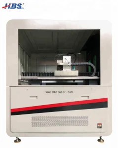
In the high-speed evolution of micro-electronics fabrication, display panel slicing, and precision optoelectronic assemblies, the requirement for high-reliability, zero-thermal-stress material separation has positioned fiber laser cutting machines as critical infrastructure. As global exporters, we witness the industry migrating away from conventional mechanical milling and routing toward non-contact, ultra-short pulse optical processing. Under the engineering custody of Hangzhou Focus Laser Co., Ltd., this document outlines the macro technological roadmaps, compliance standards, and supply-chain efficiencies that enable manufacturing enterprises to maximize processing yield while containing lifetime operational costs.
Executive Summary: Modern laser depaneling and substrate cutting require a convergence of ultra-fine beam physics, structural damping, dynamic control software, and strict compliance with the European Machinery Directive. This playbook serves as a sourcing guide and technical roadmap for procurement directors, manufacturing engineers, and operations managers worldwide.
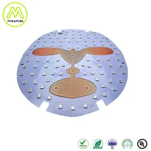
Establishment as an industry-leading OEM/ODM manufacturer specializing in micro-processing systems has enabled Hangzhou Focus Laser Co., Ltd. to design and build highly specialized machinery. The organization's core expertise lies at the intersection of precision electronics and advanced optical paths—specifically engineered for PCB laser cutting, flexible circuit board processing (FPC), semiconductor packaging, and display glass processing. Through integrating ultra-fine CNC systems, linear motor drives, and state-of-the-art fiber, picosecond, and ultraviolet laser engines, the company ensures that micro-components are processed with negligible Heat Affected Zones (HAZ) and perfectly clean edge profiles.
Equipped with a highly specialized R&D team, Hangzhou Focus Laser Co., Ltd. maintains a massive global exporting footprint, ensuring that high-precision factories in Europe, Asia, and the Americas benefit from reliable production capacity, customizable setups, and high-transmission optical setups optimized for long-term continuous shifts.
The core physics of material processing with lasers is shifting from continuous wave (CW) heating to cold ablation. The technology roadmap of Hangzhou Focus Laser relies heavily on three primary axes: Ultra-short pulse (USP) lasers, shortened optical wavelengths, and high-frequency active beam shaping.
Utilizing infrared and UV picosecond (and femtosecond) laser sources reduces the heat transfer into the substrate matrix. By delivering high peak power within picoseconds, the material undergoes sublimation directly into gas, eliminating micro-cracking and slag buildup.
By dividing the beam using spatial light modulators or diffractive optical elements (DOE), systems can cut dual lines or perform drilling tasks simultaneously, effectively doubling the yield on critical semiconductor panel lines.
On-the-fly trajectory calculations adjust scanning speed dynamically at corners and curves. This protects thinner substrate margins, preventing heat buildup at high deceleration zones.
Looking forward, the roadmap integrates fiber lasers operating at higher power levels with beam quality factors ($M^2$) approaching the diffraction limit ($< 1.1$). This guarantees that the energy remains tightly concentrated, reducing the kerf width to under 15 microns. This level of control is essential for processing the high-density interconnects (HDI) found in next-generation smartphone circuit boards and advanced packaging modules.
The industrial landscape requires laser systems that are not single-purpose tools, but integrated solutions capable of processing complex materials. Hangzhou Focus Laser addresses multiple critical sectors with tailor-made optical parameters:
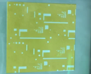
Mechanical routers exert physical stress on components placed near the edge of circuit boards, causing capacitor cracking and solder joint failures. Our high-precision PCB depaneling systems use UV picosecond lasers to cut through FR4, polyimide coverlay, and copper traces with zero vibration, eliminating delamination risk and mechanical failures.
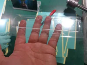
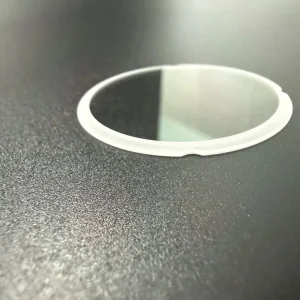
Slicing tempered glass, sapphire optical components, and multi-layer display panels requires ultra-short infrared pulses. Our infrared picosecond laser systems create controlled micro-voids in the glass structure, allowing clean cleavage without micro-cracks or the need for secondary grinding stages. This process is essential for smartphone screens and high-resolution instrumentation optics.
The transition to EV battery configurations and Silicon Carbide (SiC) modules requires cutting highly conductive and wear-resistant substrates. By configuring lasers with high-power pulses, our tools process advanced materials like copper foils, aluminum tabs, and raw SiC matrices with high throughput, ensuring smooth interfaces that optimize electrical connectivity.
| Laser Configuration | Wavelength | Target Materials | Primary Industry Application | Max Heat Affected Zone (HAZ) |
|---|---|---|---|---|
| UV Picosecond | 355 nm | Polyimide, PCB, FPC, MEMS Lenses | High-density Electronics & Micro-sensors | < 5 μm |
| IR Picosecond | 1064 nm | Sapphire Glass, Display Panels, Ceramics | Consumer Devices & Optical Instrumentation | < 10 μm |
| High-Power CO2 | 10.6 μm | Thick Acrylics, Glass Tubes, Organic Fibers | Industrial Engraving & Structural Separation | < 50 μm |
| High-Performance Fiber | 1070 nm | Stainless Steel, Copper, Aluminum | Automotive, Battery Assembly & Metal Fab | < 15 μm |
Exporting industrial laser systems to strict regulatory regions like the European Union and North America requires strict adherence to international standards. Standard machinery clearances are insufficient for Class 4 laser installations.
Our entire fiber and picosecond laser catalog is CE Certified, complying with all necessary directives:
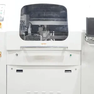
Beyond design compliance, global operations require localized field service. Hangzhou Focus Laser maintains a responsive support system, providing field engineers for installation, calibration, and training. We offer remote telemetry diagnostics to assist your on-site engineering team, troubleshooting beam alignment and PLC logic in real time to minimize downtime.
Manufacturing high-precision optical equipment requires a resilient and integrated supply chain. Operating from our production base in Hangzhou, China, Hangzhou Focus Laser utilizes a highly integrated manufacturing cluster that brings together optics suppliers, structural metal casting foundries, and CNC controller developers in close geographic proximity.
This integration provides several key operational advantages:
Procurement directors must look beyond the initial purchase price of laser cutting machinery. A comprehensive TCO assessment includes long-term consumables, power conversion efficiency, gas consumption, and maintenance schedules.
Our fiber laser systems are engineered to optimize these operational costs:
Get professional, engineering-grade answers regarding optical paths, materials, machine calibration, and delivery.
UV lasers (355 nm) operate primarily via cold ablation, where high-energy photons break molecular bonds directly without generating significant heat. Infrared lasers (1064 nm) rely on thermal melting. Because PCB and FPC boards contain sensitive polymers, adhesives, and thin copper layers, the thermal stress from an IR laser can lead to delamination, charring, and increased Heat Affected Zones (HAZ). UV lasers deliver exceptionally clean cuts with minimal thermal impact.
All our exported laser machines are fully CE certified. They comply with the Machinery Directive 2006/42/EC, Low Voltage Directive 2014/35/EU, and EMC Directive 2014/30/EU. Critically, we design according to EN 60825-1 laser safety standards, utilizing a fully interlocked Class 1 light-tight enclosure with laser-rated viewing windows to protect operators from exposure.
Our quality assurance protocol includes a 72-hour continuous burn-in and cycling test. We run full laser-power stability tests using calibrated power meters, verify optical path alignment using helium-neon guide lasers, and check axis positioning accuracy using laser interferometers. A final test cut is performed on sample materials provided by the client, with cut quality verified under scanning electron microscopes before shipping authorization.
Standard machine configurations are typically shipped within 30 to 45 business days from order confirmation. For customized ODM/OEM systems, lead times range from 60 to 75 days. All machinery is packed in vacuum-sealed moisture barrier bags with silica desiccant, enclosed in export-grade fumigated wooden crates with integrated shock-absorbing skids to ensure protection during ocean transit.
Yes, our systems are built for round-the-clock industrial use. They feature cast gantry frames for thermal stability, industrial-grade linear motors, and closed-loop liquid chillers. The laser diodes are rated for up to 100,000 hours of operation, making them suitable for high-volume manufacturing environments.
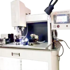
Our high-precision systems use an active autofocus sensor and a dynamic focal tracking system. The optical head continuously monitors the physical distance to the substrate using optical or capacitive sensors, adjusting the focus axis dynamically within microseconds to maintain a consistent spot size across the entire working area.
Complete your facility setup with our specialized optical, alignment, and laser machining systems.
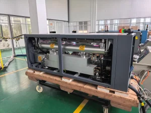
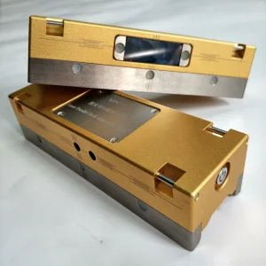
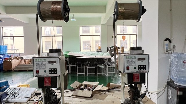
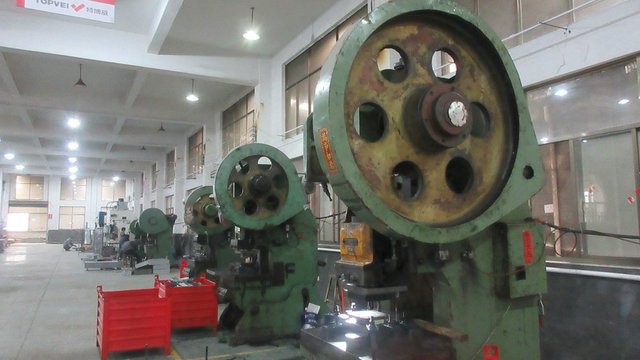
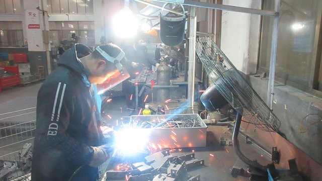
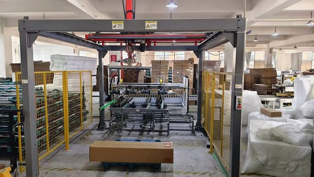
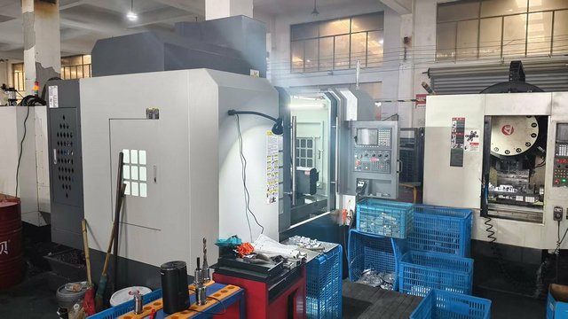
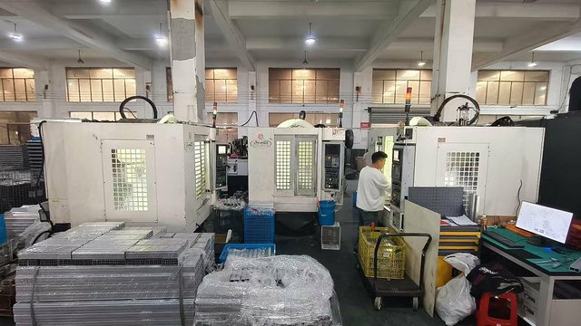
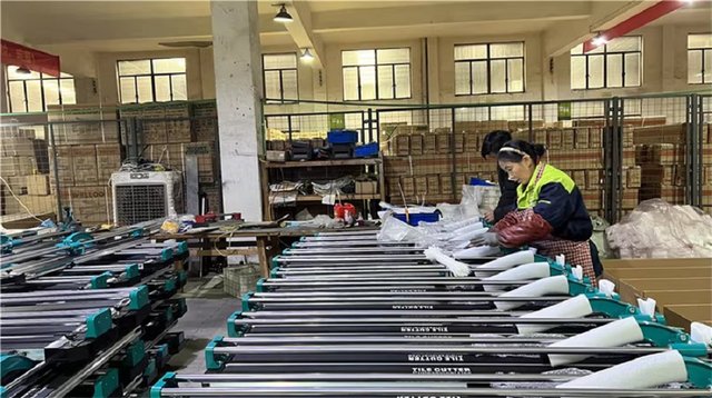
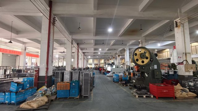
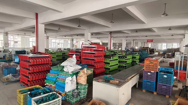
Visual documentation from our manufacturing floor and specialized component assembly lines.