Explore our core technologies optimized for the demanding semiconductor and precision engineering landscape of Tokyo's industrial hubs.
As a leading Semiconductor Packaging Laser Cutting Solutions Exporter in Tokyo, we recognize the critical role that the Japanese capital plays in the global silicon supply chain. Tokyo is not just a commercial hub; it is the heart of high-precision engineering where "Monozukuri" (the art of making things) meets 21st-century AI technology.
In the districts of Minato, Ota, and the surrounding Kanto region, the density of semiconductor material suppliers and equipment manufacturers is unparalleled. The demand for precision laser cutting in semiconductor packaging has skyrocketed as chips become smaller, more complex, and vertically integrated (3D Packaging). Our role as a Tokyo-focused exporter is to bridge the gap between world-class laser technology and the rigorous yield requirements of Japanese fabless and IDM giants.
The industry is shifting from traditional mechanical sawing to advanced laser solutions. In Tokyo’s tech corridors, three major trends are defining the future of Semiconductor Packaging:
1. Heterogeneous Integration: Combining multiple components into a single package requires laser cutting that can handle different materials (silicon, ceramics, polymers) without thermal damage. Our ultra-fine beam control technology ensures zero-stress processing.
2. Sustainability & Green Manufacturing: Tokyo’s strict environmental regulations have pushed manufacturers to adopt laser processes that eliminate the need for cooling water and chemical slurries, significantly reducing the carbon footprint of PCB depaneling.
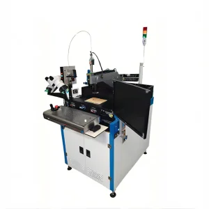
3. AI-Driven Quality Control: Modern exporters in Tokyo are integrating Deep Learning vision systems into laser machines to detect micro-cracks in real-time. This "Smart Factory" approach is essential for maintaining the 99.99% yield rates required in automotive and medical electronics.
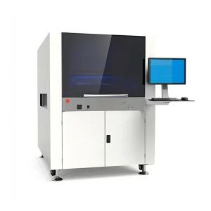
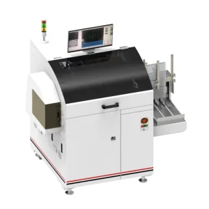
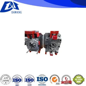
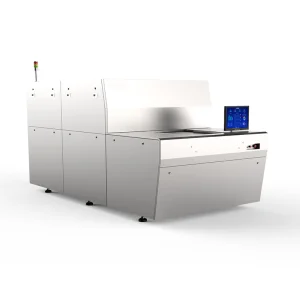
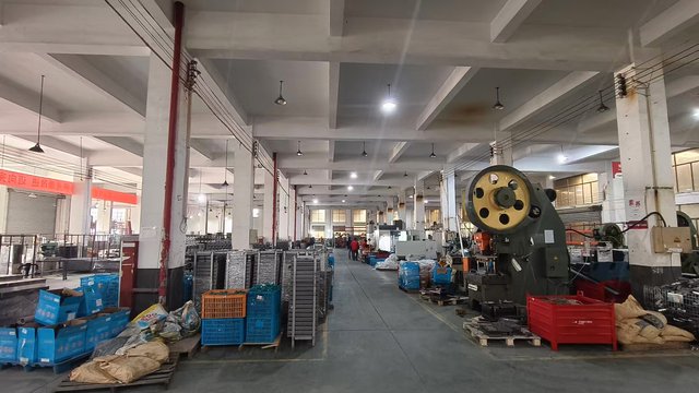
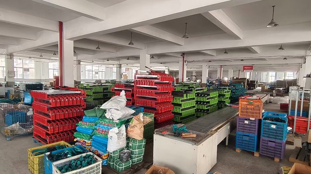
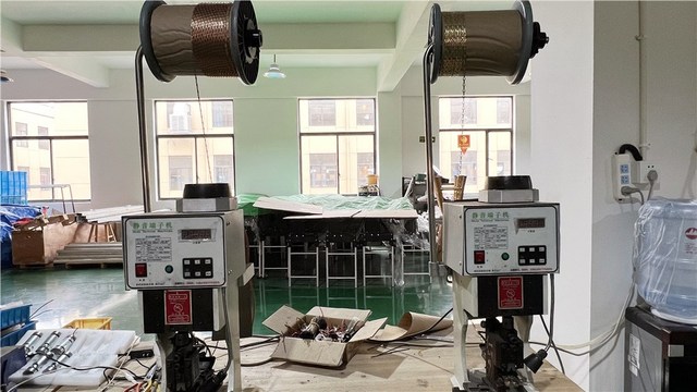
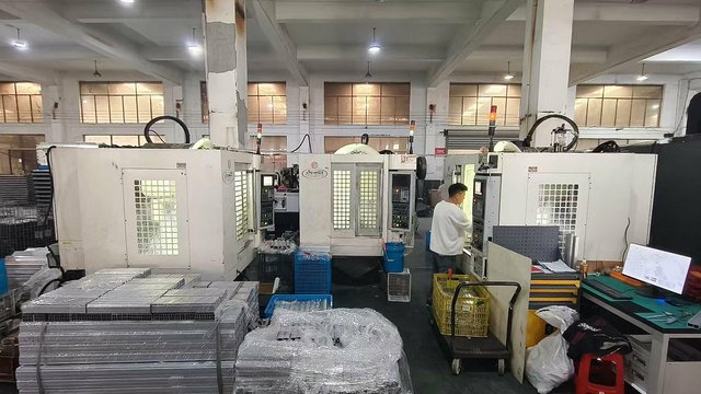
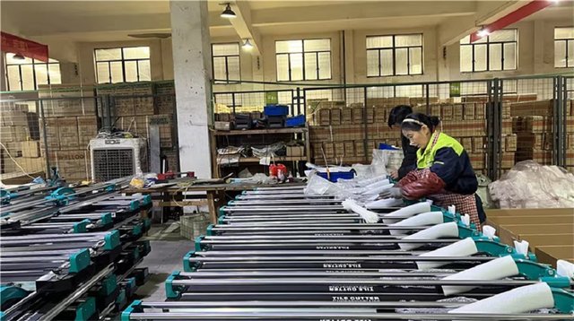
Hangzhou Focus Laser Co., Ltd. is a professional manufacturer specializing in advanced laser processing equipment for the electronics and display industries. The company focuses on the development and production of PCB laser cutting machines and glass laser cutting systems, delivering high-precision solutions for micro-electronics manufacturing and optical material processing.
Its technologies are widely applied in PCB depaneling, flexible circuit board processing, semiconductor packaging, and precision glass cutting for smartphones, display panels, and optical components. By integrating fiber laser technology, ultra-fine beam control, and intelligent CNC systems, Hangzhou Focus Laser ensures high cutting accuracy, smooth edges, and minimal thermal damage during processing.
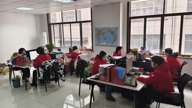
The company’s equipment is extensively used in industries such as consumer electronics, semiconductor manufacturing, automotive electronics, and smart display production. It supports both high-volume industrial production and customized precision machining requirements. Hangzhou Focus Laser Co., Ltd. emphasizes innovation, reliability, and engineering excellence. With strong R&D capabilities and strict quality control standards, the company provides OEM and ODM services to meet global customer needs, particularly as a key exporter for Tokyo-based technical projects.
Tokyo’s industrial landscape is unique, requiring solutions that fit compact, high-efficiency urban factories. Our Semiconductor Packaging Laser Cutting Solutions are utilized in several key local scenarios:
With Japan's shift toward EVs, our laser systems provide precision cutting for SiC and GaN power modules in suburban Tokyo production lines.
High-frequency PCB processing for Tokyo’s telecommunications network expansion, ensuring zero signal interference.
Supporting Ota City’s medical equipment cluster with micro-machining for surgical sensors and implants.
Enabling the miniaturization of wearables and smart home devices for the competitive Tokyo retail market.
We combine Japanese engineering standards with global cost-efficiency, ensuring that every laser machine exported meets the "Tokyo Quality" benchmark. Our R&D focuses on the thermal-mechanical stability needed for high-speed semiconductor throughput.
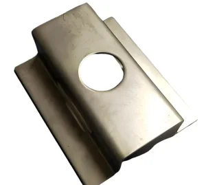
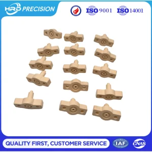
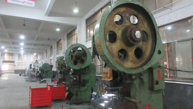
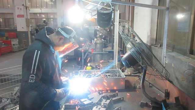
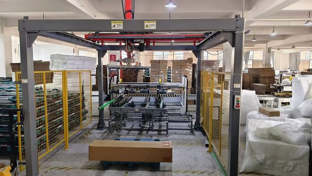
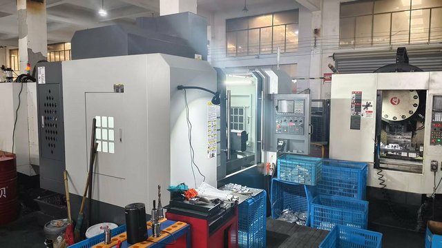
Comprehensive manufacturing solutions ranging from medical-grade precision to automotive-strength fabrication.
In conclusion, whether you are looking for a reliable Semiconductor Packaging Laser Cutting Solutions Exporter in Tokyo for high-volume production or a specialized R&D partner, our technologies provide the precision, speed, and reliability required to succeed in the competitive global market. From ultra-high purity gas solutions to deep learning vision inspection, we cover every aspect of the modern semiconductor manufacturing cycle.