
1 / 5
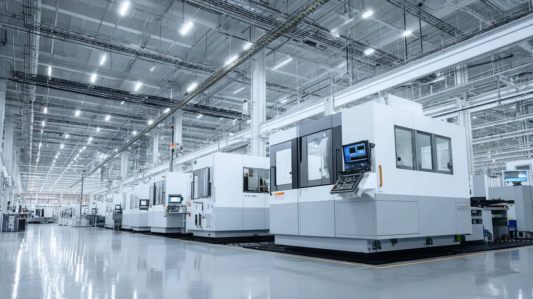
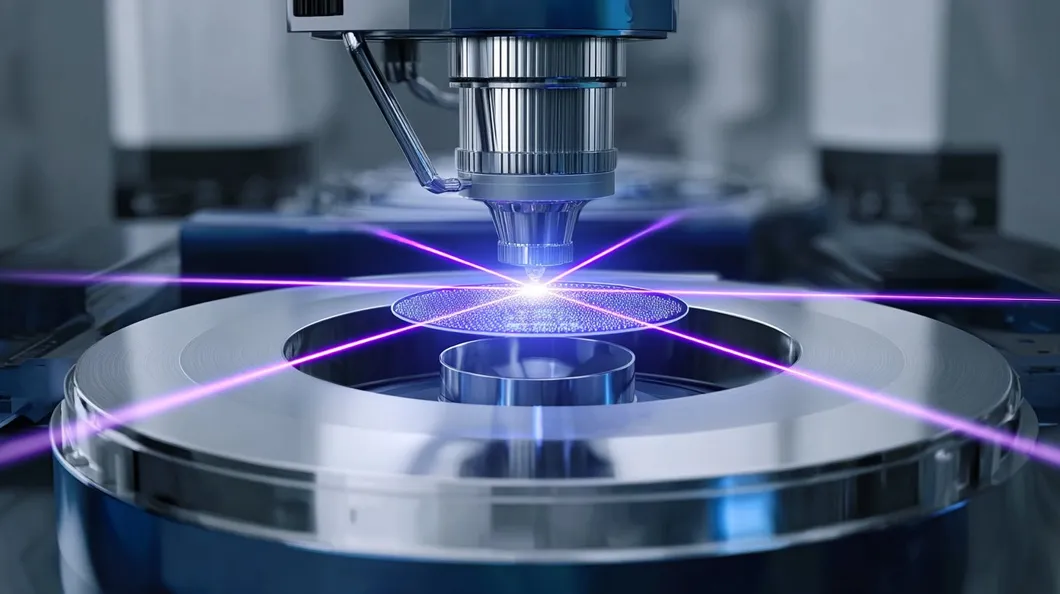
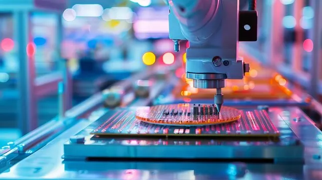
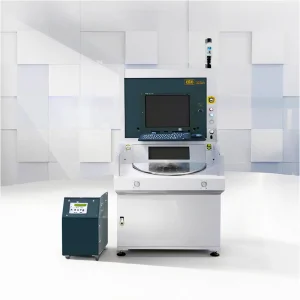
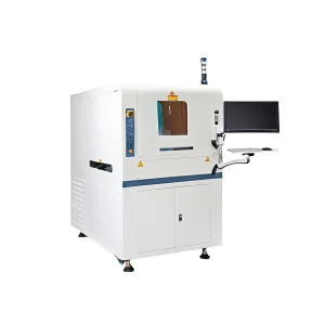
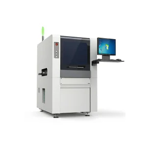
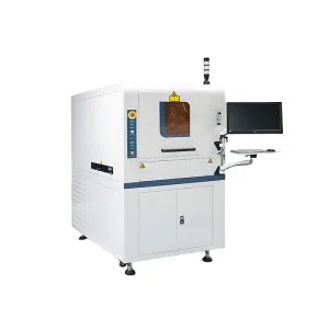
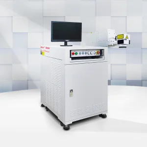
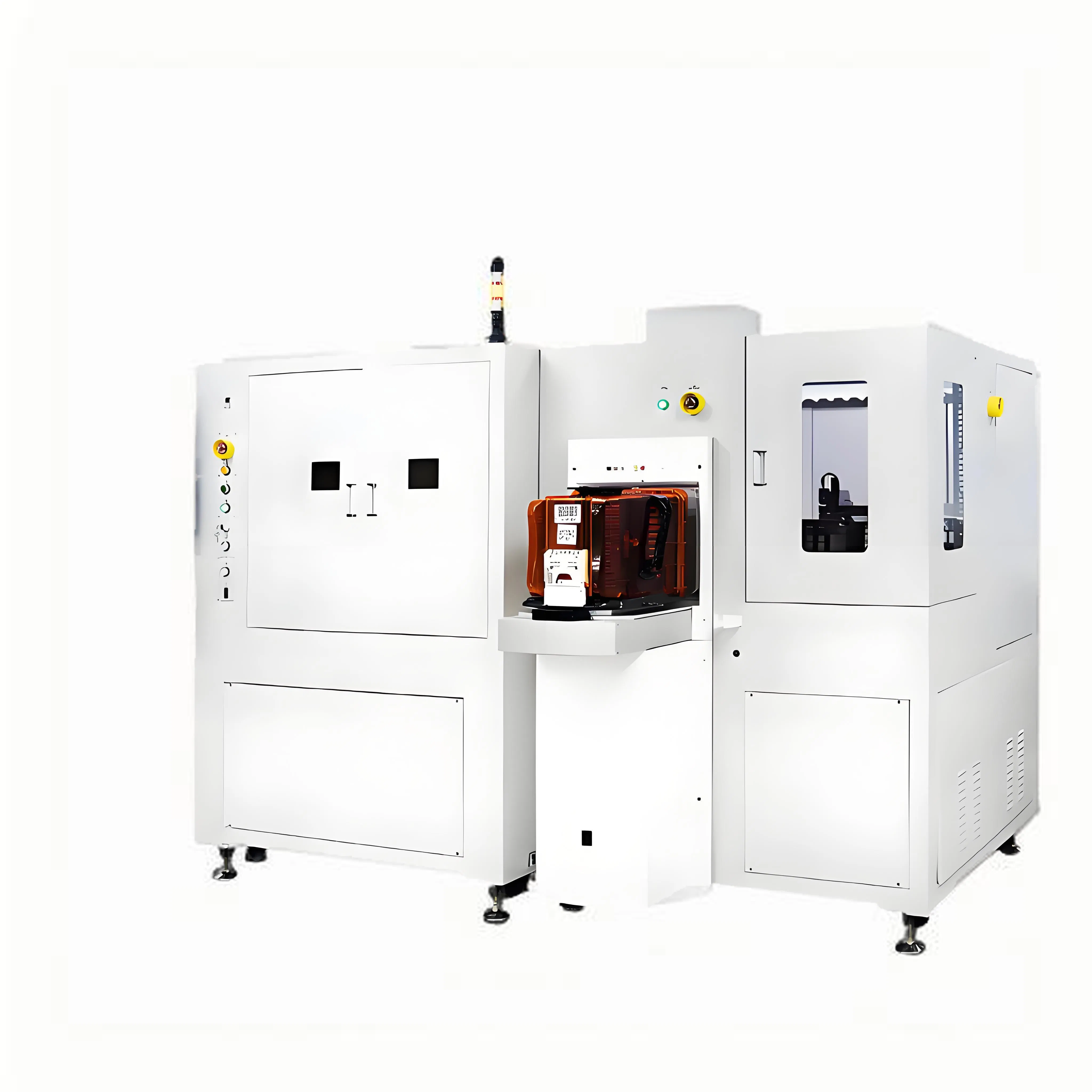
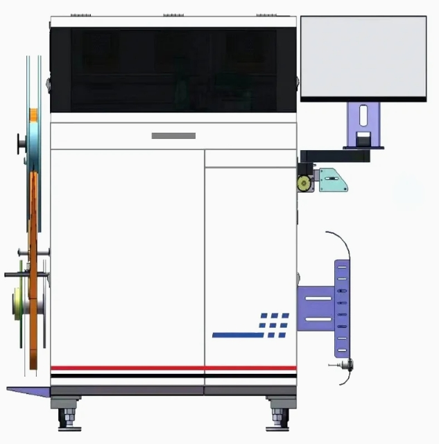
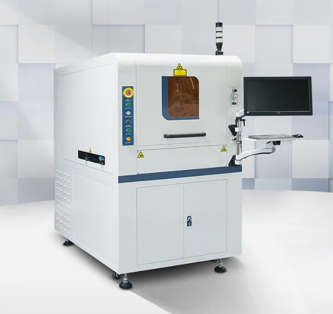
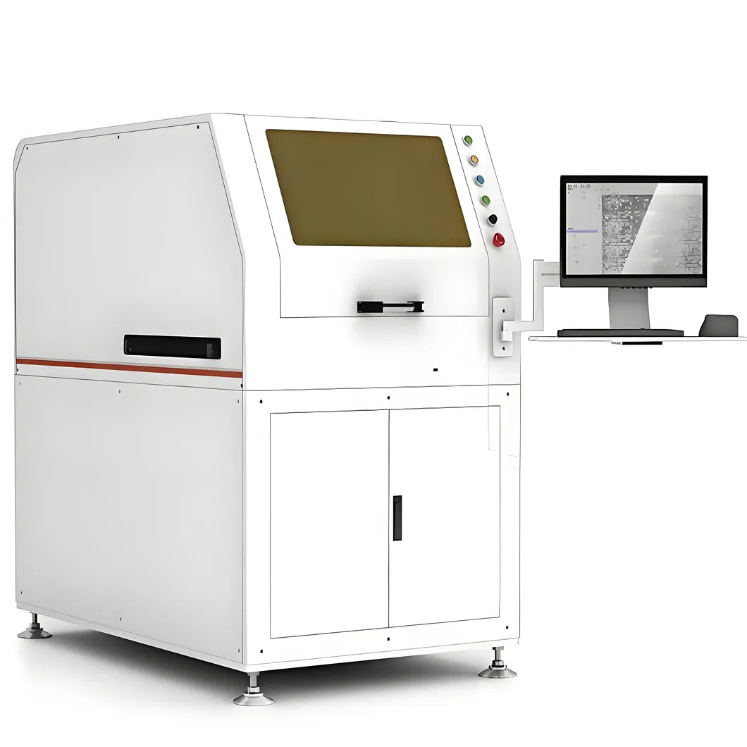
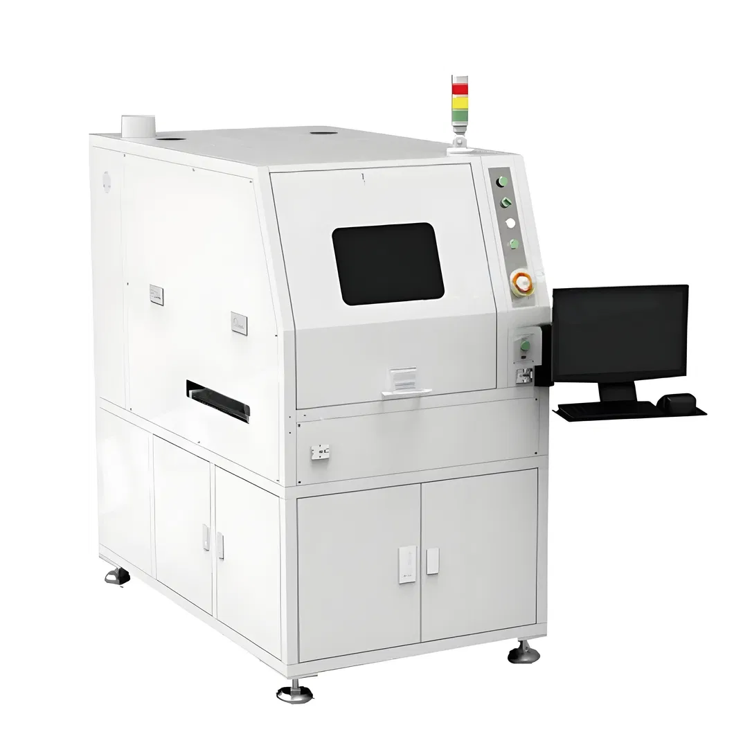
High Quality PCB Laser Marking System
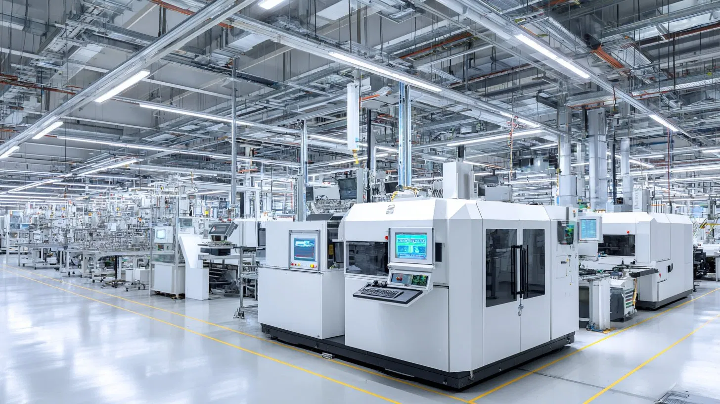
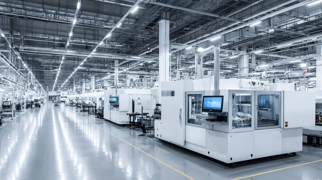
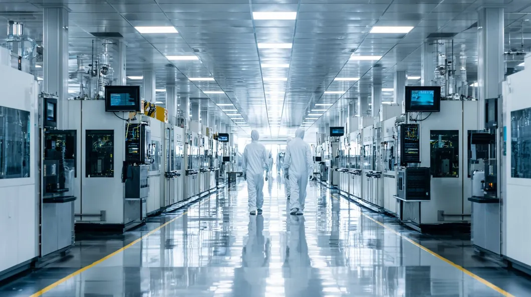
This system realizes fully automatic online dynamic marking for the PCB industry, and achieves fully automatic loading and unloading through the SMEMA standard interface.
核心特点 Features:
| Laser Type | Scan Range | Max Power Consumption | Operating Height | Sample Size | Dimensions | Weight |
|---|---|---|---|---|---|---|
| Fiber / Green / UV / CO2 | 50x50mm² (customizable) | 2.5kW | 900±20mm | 50x50mm²-460x510mm² | 1000x600x1700mm³ | Less than 1.5 tons |
Pioneering advanced semiconductor equipment with 10+ patents, evolving for emerging tech nodes.
ISO 9001 & CE certified manufacturing, ensuring precision (±5µm) and reliability.
24/7 technical assistance + on-site training, minimizing downtime and maximizing yield.
Efficient global shipments to 30+ countries with full customs documentation.
Key Technical Features:
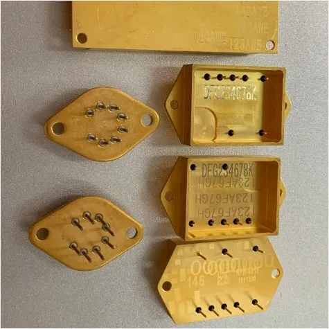
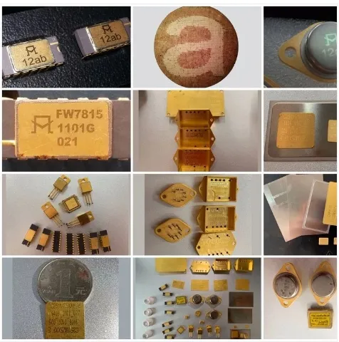
• Electronics: PCB/wafer traceability
• Metal: Deep engraving
• Medical: Biocompatible marking