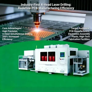
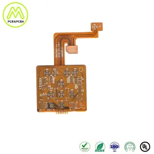
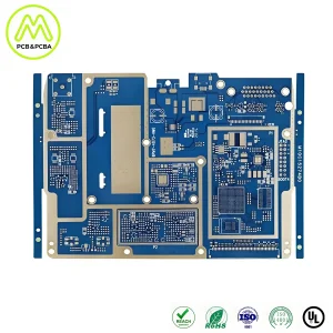
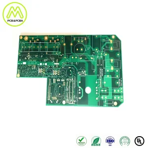
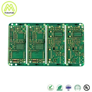
The global electronics landscape is undergoing a paradigm shift. As we transition into the era of 5G, Artificial Intelligence (AI), and the Internet of Things (IoT), the demand for High-Density Interconnect (HDI) PCBs has skyrocketed. Unlike traditional PCBs, HDI boards utilize micro-via technology, finer lines, and smaller spaces to achieve higher circuit density. This miniaturization is impossible without advanced Laser Processing.
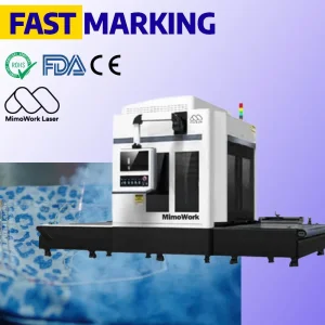
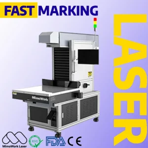
Currently, the industrial world relies on laser technology for drilling, cutting, and marking PCBs with sub-micron precision. In regions like North America, Europe, and East Asia, the automotive and medical sectors are demanding more robust and compact electronic assemblies. This has placed laser processing at the heart of the modern industrial supply chain, where mechanical drilling can no longer meet the physical limits of new dielectric materials.
The trajectory of HDI PCB laser processing is defined by three key trends: Automation, Integration, and Sustainable Precision.
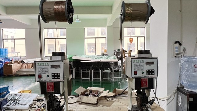
1. mSAP (Modified Semi-Additive Process): As circuit lines shrink below 30μm, laser systems are being integrated with chemical plating processes to create ultra-fine patterns.
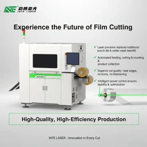
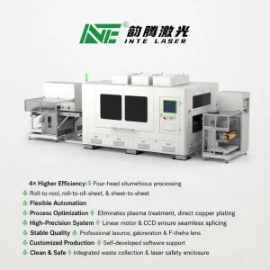
2. Roll-to-Roll (R2R) Processing: For flexible PCBs (FPC), R2R laser systems are the gold standard, offering unmatched throughput and material efficiency.
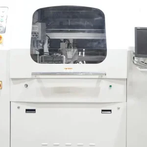
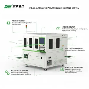
3. AI-Driven Vision Systems: Modern machines now incorporate "Smart Eyes"—high-resolution cameras combined with AI algorithms to detect board warping and adjust the laser path in real-time, ensuring zero-defect manufacturing.
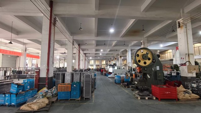
China has evolved from a high-volume manufacturer to a global R&D powerhouse in laser technology. Buying from a leading Chinese factory like Hangzhou Focus Laser Co., Ltd. offers several strategic advantages:
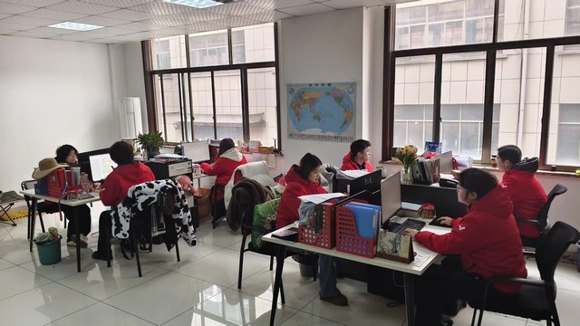
We are located in the heart of the electronics manufacturing hub, ensuring rapid access to the latest components and materials.
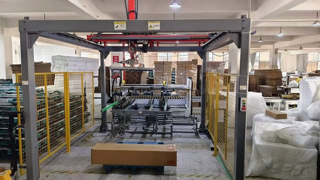
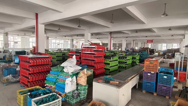
Through optimized production and scaled manufacturing, we provide high-end laser systems at a competitive ROI for global buyers.
Our engineering teams can customize hardware and software (OEM/ODM) faster than traditional Western suppliers.
Experience & Expertise: With decades of combined engineering experience, our team specializes in the interaction between laser beams and substrate materials (FR4, Polyimide, Ceramics). We don't just sell machines; we provide process parameters that ensure your production starts on day one.
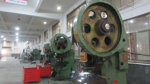
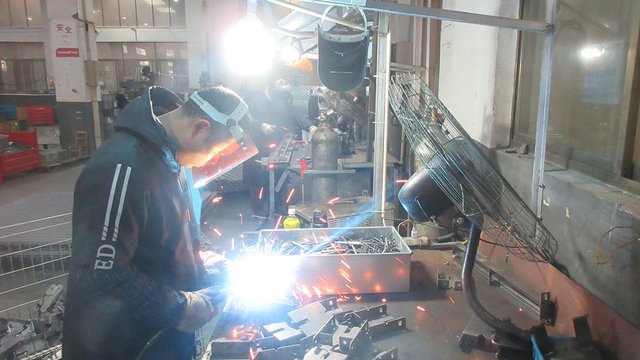
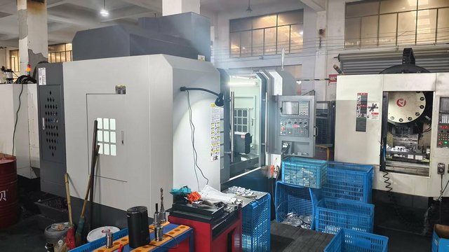
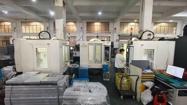
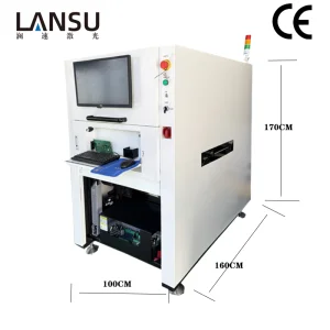
Authoritativeness & Trust: Hangzhou Focus Laser Co., Ltd. is a professional manufacturer specializing in advanced laser processing equipment for the electronics and display industries. The company focuses on the development and production of PCB laser cutting machines and glass laser cutting systems, delivering high-precision solutions for micro-electronics manufacturing and optical material processing.
Our technologies are widely applied in PCB depaneling, flexible circuit board processing, semiconductor packaging, and precision glass cutting for smartphones, display panels, and optical components. By integrating fiber laser technology, ultra-fine beam control, and intelligent CNC systems, we ensure high cutting accuracy, smooth edges, and minimal thermal damage.
Procuring industrial laser equipment requires a partner who understands international standards (CE, UL, FDA). Global buyers from the USA, Germany, Japan, and Vietnam seek our equipment for localized applications such as:
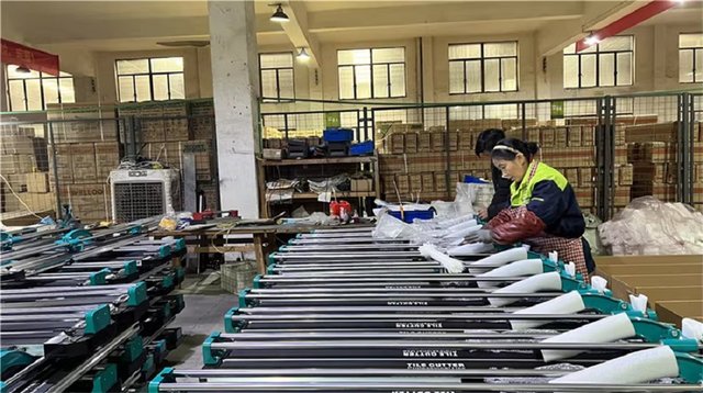
We support global exporters by providing robust packaging, remote installation support, and multilingual software interfaces, making our "Made in China" technology a global asset.