Explore our core engineering portfolio of advanced glass dicing, wafer processing, and PCB separation systems configured for modern high-yield smart factories.
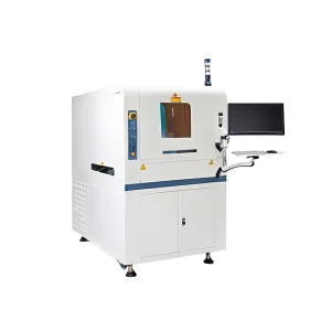
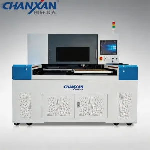
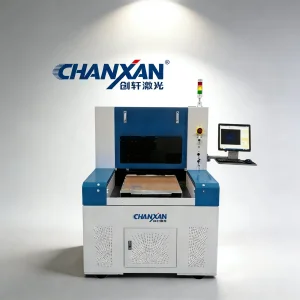
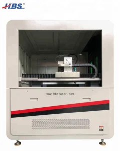
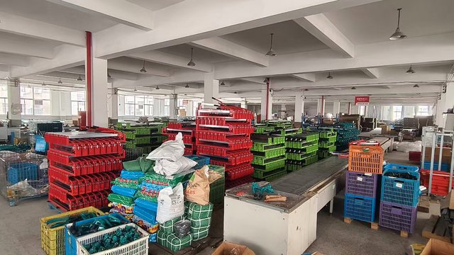
In the rapidly evolving world of electronics manufacturing, precision is no longer just an advantage—it is an absolute prerequisite. As a specialized engineering powerhouse, Hangzhou Focus Laser Co., Ltd. stands at the forefront of this industrial revolution. The company is a professional manufacturer specializing in advanced laser processing equipment tailored primarily for the microelectronics, 3C display, and semiconductor industries. By integrating cutting-edge fiber lasers, picosecond and femtosecond pulse control platforms, and ultra-high-speed CNC linear motion modules, Hangzhou Focus Laser achieves microns-level machining tolerance with minimal thermal footprint.
Our developmental efforts center around two critical technology branches: PCB laser cutting systems and precision glass laser splitting/dicing machines. In contrast to conventional mechanical tooling methods—which introduce mechanical stress, microscopic fracturing, and tooling wear—our non-contact laser process provides sub-50µm edge accuracy, burr-free profiles, and unmatched repeat accuracy. These performance vectors are critical for flexible circuits (FPCs), high-density interconnect (HDI) substrates, and brittle optical components used in aerospace, consumer electronics, and high-pressure deep sea enclosures.
High-speed UV/Green laser source configures for low-thermal stress separation of rigid-flex boards without damaging adjacent surface-mount components.
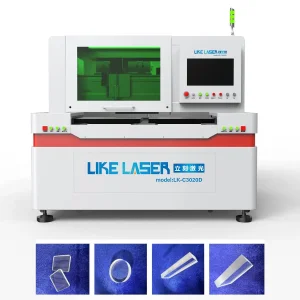
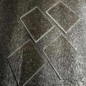
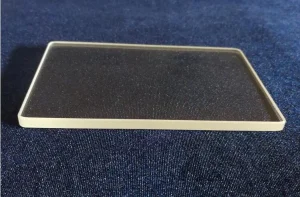
Utilizes ultra-fast infrared and picosecond lasers to split displays, cover glass, and sapphire windows with clean, micro-crack-free vertical sidewalls.
Innovative optical focus networks optimized for SiC (Silicon Carbide) wafer dicing and thin-wafer microprocessing to maximize yield.
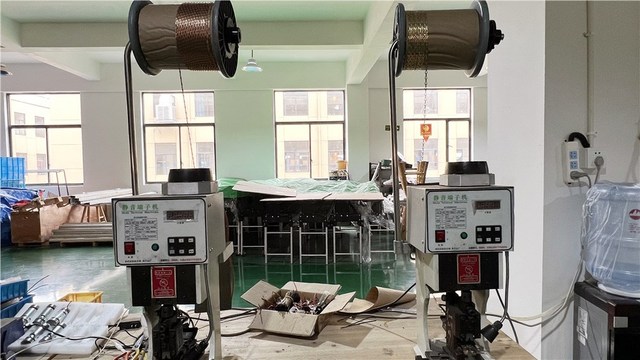
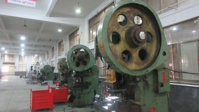
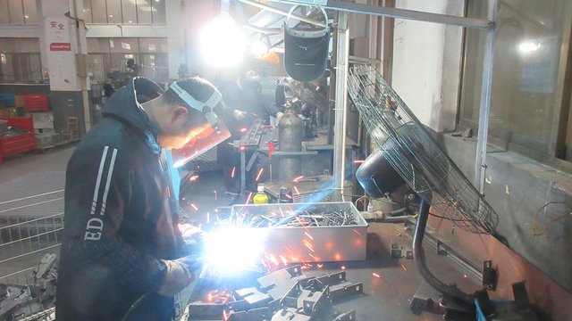
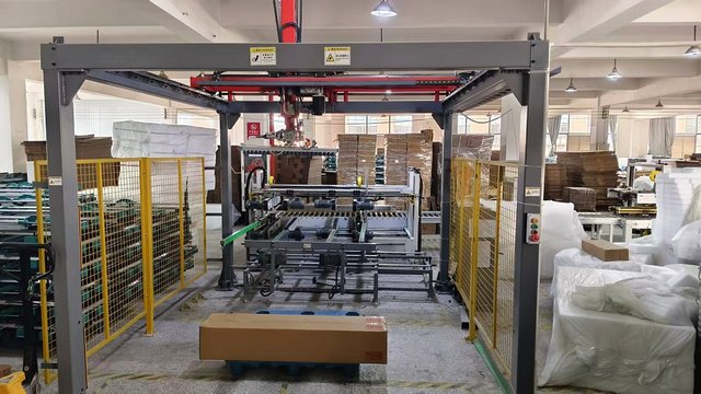
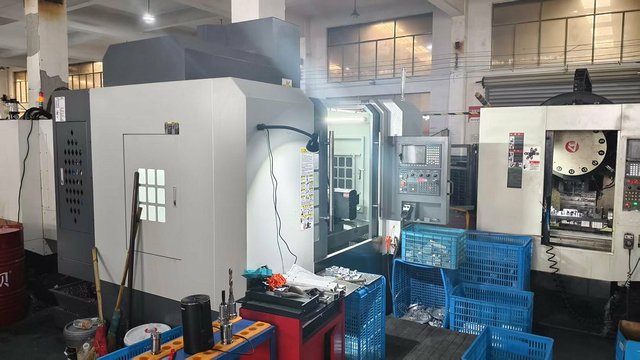
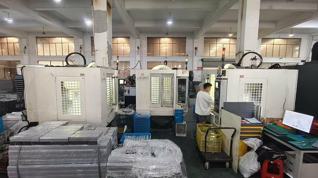
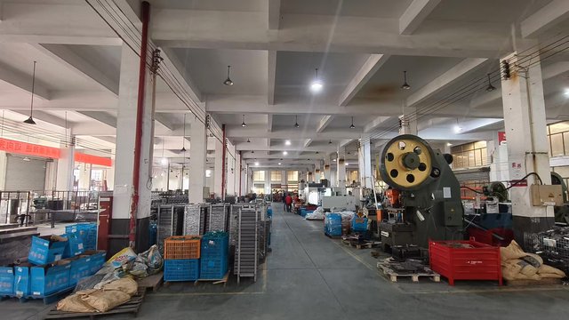
The global competitiveness of China-based laser machine suppliers is built upon a fully integrated component and software supply ecosystem. In the Yangtze River Delta manufacturing cluster, Hangzhou Focus Laser coordinates with regional industry giants, specialized optic houses, and CNC system developers (such as Estun Technology) to construct high-reliability machines at optimized cycles. This ecosystem eliminates the long lead times common with European and North American integrators while guaranteeing access to the latest optical innovations.
By maintaining complete control over our design, CNC configuration, and component procurement, we can adapt configurations rapidly for bespoke industrial projects. Our suppliers must meet stringent ISO 9001 and ISO 14001 guidelines, and every optical element—from the high-speed galvo-scanners to telecentric lenses—is subject to detailed performance checks before system integration. This cluster effect results in highly dynamic ODM/OEM support, shorter time-to-market, and a highly competitive performance-to-price ratio.
Procurement teams and optical design engineers from international electronics brands evaluate laser processing hardware on several core parameters: beam quality factor (M²), heat-affected zone (HAZ), throughput speed, and automation integration capabilities. Achieving clean microprocessing is highly dependent on managing pulse duration and wavelength. Shorter wavelengths (such as 355nm UV) and shorter pulse widths (picosecond and femtosecond regimes) minimize thermal effects by vaporizing materials directly through photo-ablation rather than melt-expulsion.
Below is a detailed technical matrix comparing standard industrial systems to guide sourcing decisions based on material requirements and production volumes:
| System Type | Wavelength / Laser Source | Pulse Width / Speed | Target Materials | Key Advantages |
|---|---|---|---|---|
| UV Laser Marking/Cutting | 355nm UV Solid-State | <15 ns / Up to 15,000 mm/s | Polymers, Glass, PCB Coverlays | Cold ablation, minimal carbonization, burr-free |
| Picosecond Glass Splitting | 1064nm / 532nm Ultrafast | <10 ps / Up to 8,000 mm/s | Display Glass, Sapphire, Quartz | No micro-cracking, clean vertical edges, fast processing |
| Green Laser Wafer Dicing | 532nm Green Gas/Solid | <12 ns / High Repetition | SiC Wafer, Silicon Wafers | Excellent absorption, high throughput on thin substrates |
| CO2 Fast Flow Systems | 10.6um Carbon Dioxide | Continuous Wave (CW) / Pulsed | Thick Glass, Acrylic, Organic Materials | High thermal volume cutting, robust industrial reliability |
Industrial applications for precision laser systems require custom optics configurations tailored to the material's physical properties. Our engineering database details the physical behaviors of various materials under laser processing, demonstrating Hangzhou Focus Laser's capability to deliver optimized solutions across challenging application environments:
Smartphones and smart-wearable displays require high-precision glass cutting and contour separation. Our picosecond laser glass cutting lines achieve smooth, clean edges on multi-layered displays with no delamination or micro-cracks, ensuring high durability for structural components.
Sapphire components used in high-pressure deep water vessels require exceptional mechanical strength and edge quality. Mechanical grinding often leaves sub-surface damage that can lead to failure under pressure. Our ultrafast picosecond system cuts these materials with precise edge angles, maintaining high structural integrity.
Instruments used in space applications depend on wear- and chemical-resistant glass windows. Working with these hard glasses requires precise processing without inducing residual thermal stress. Our integrated systems allow clean vertical separation, meeting strict aerospace compliance standards.
For global buyers, purchasing heavy equipment from international suppliers involves verifying quality standards and ensuring long-term technical support. Hangzhou Focus Laser addresses these concerns with comprehensive certification alignments and structured local support networks:
International Standards Compliance: All export-grade machines are engineered to meet CE directives (Low Voltage and Electromagnetic Compatibility), FDA CDRH laser safety standards (Class I fully enclosed configurations), and UL/CSA electrical design specifications. Our enclosures feature interlocked access panels, active optical path shielding, and integrated extraction ports to maintain safe operating environments.
Global Technical Support Model: We maintain overseas field engineering partnerships and localized distributor networks to provide installation, operator training, and field support. For rapid troubleshooting, our systems feature secure remote diagnostic interfaces that allow our software engineering team to perform system checks, adjust galvo calibration files, and update CNC firmware remotely. Additionally, our key wear-parts depots in North America, Europe, and Southeast Asia ensure minimal downtime for critical manufacturing lines.
The precision laser micromachining industry is moving toward shorter pulse durations, hybrid optical configurations, and increased integration of artificial intelligence. In display manufacturing, the transition from LCD to OLED and micro-LED displays requires advanced systems capable of cutting glass, polymer layers, and metallic trace structures simultaneously. This demand is driving the development of multi-wavelength platforms that switch dynamically between infrared, green, and ultraviolet modes to process composite materials efficiently.
Additionally, integrating real-time optical coherence tomography (OCT) allows systems to perform active depth tracking and auto-focus adjustments during dicing. This technology enables the system to adapt dynamically to wafer warping and material variations, protecting components from micro-fractures. Machine learning diagnostics are also becoming standard, monitoring optical power stability and axis acceleration to predict component wear and schedule preventive maintenance, reducing unplanned downtime.

Expert engineering insights regarding laser processing parameters, material limitations, and integration logistics.
The difference lies in the material ablation mechanism. UV lasers (355nm) operate primarily via photo-chemical ablation ("cold processing"), where high-energy photons break chemical bonds directly, resulting in minimal heat generation. Picosecond lasers (whether green or infrared) utilize ultra-short pulse durations (typically <10-12 picoseconds) to vaporize material through photo-physical ablation. Because the pulse duration is shorter than the thermal diffusion time of most materials, the energy is concentrated and vaporizes the target before heat can travel to the surrounding area, making it effective for hard, brittle materials like sapphire and cover glass.
We manage the HAZ through a combination of ultra-short pulse laser sources, specialized telecentric scan lenses, and dynamic galvo control algorithms. By optimizing parameters such as hatch spacing, feed speed (up to 12,000 mm/s), and pulse repetition rate, our systems prevent heat accumulation. This maintains the Heat Affected Zone below 15-20µm, protecting sensitive surface-mount components located close to the cut line.
Yes. Our multi-axis CNC glass laser processing systems are designed to accommodate 3D curved surfaces and multi-layered configurations (glass + polarizer + adhesive). We utilize high-speed z-axis focal tracking systems and custom optical beam shaping (Bessel beams) to ensure uniform laser energy density through the material profile. This allows for clean, single-pass splitting of layered panel assemblies without causing delamination.
Estun Technology provides high-resolution servo drives and motion controllers that link directly with our laser pulsing controls. This enables accurate synchronization, adjusting the laser pulse rate automatically during acceleration or deceleration. This prevents energy concentration at corners, ensuring consistent cut depth and width across complex paths.
Each system undergoes a 72-hour factory testing cycle before shipment. Upon arrival, our local service partners or factory engineers support the installation and onsite calibration. We provide comprehensive operator training covering optical alignment, laser safety, and parameter optimization. For ongoing support, our remote diagnostics allow real-time analysis of software and system parameters.
Complete your facility integration with our high-power cleaning systems, ultrafast wafer dicers, and specialized optical protective layers.
 Focus Laser